|
Motor de Búsqueda de Datasheet de Componentes Electrónicos |
|
|
Motor de Búsqueda de Datasheet de Componentes Electrónicos |
|
ATtiny44 Datasheet(PDF) 63 Page - ATMEL Corporation |
|
|
|||||||||||||||||||||||||||||
ATtiny44 Datasheet(HTML) 63 Page - ATMEL Corporation |
|
|
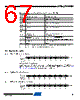
63 / 236 page  63 8006H–AVR–10/09 ATtiny24/44/84 • Port A, Bit 6 – ADC6/DI/SDA/MOSI/OC1A/PCINT6 • ADC6: Analog to Digital Converter, Channel 6. • SDA: Two-wire mode Serial Interface Data. • DI: Data Input in USI Three-wire mode. USI Three-wire mode does not override normal port functions, so pin must be configure as an input for DI function. • MOSI: Master Data output, Slave Data input for SPI channel. When the SPI is enabled as a Slave, this pin is configured as an input regardless of the setting of DDA6. When the SPI is enabled as a Master, the data direction of this pin is controlled by DDA6. When the pin is forced by the SPI to be an input, the pull-up can still be controlled by the PORTA6 bit. • OC1A, Output Compare Match output: The PA6 pin can serve as an external output for the Timer/Counter1 Compare Match A. The pin has to be configured as an output (DDA6 set (one)) to serve this function. This is also the output pin for the PWM mode timer function. •PCINT6: Pin Change Interrupt source 6. The PA6 pin can serve as an external interrupt source for pin change interrupt 0. • Port A, Bit 7 – ADC7/OC0B/ICP1/PCINT7 • ADC7: Analog to Digital Converter, Channel 7. • OC0B, Output Compare Match output: The PA7 pin can serve as an external output for the Timer/Counter0 Compare Match B. The pin has to be configured as an output (DDA7 set (one)) to serve this function. This is also the output pin for the PWM mode timer function. • ICP1, Input Capture Pin: The PA7 pin can act as an Input Capture Pin for Timer/Counter1. •PCINT7: Pin Change Interrupt source 7. The PA7 pin can serve as an external interrupt source for pin change interrupt 0. Table 10-4 and Table 10-6 relate the alternate functions of Port A to the overriding signals shown in Figure 10-5 on page 59. Table 10-4. Overriding Signals for Alternate Functions in PA7..PA5 Signal Name PA7/ADC7/OC0B/ICP1/ PCINT7 PA6/ADC6/DI/SDA/MOSI/ OC1A/ PCINT6 PA5/ADC5/MISO/DO/ OC1B/ PCINT5 PUOE 0 0 0 PUOV 0 0 0 DDOE 0 USIWM1 0 DDOV 0 (SDA + PORTA6) • DDA6 0 PVOE OC0B enable (USIWM1 • DDA6) + OC1A enable (USIWM1 • USIWM0) + OC1B enable PVOV OC0B ( USIWM1• DDA6) • OC1A USIWM1 • USIWM0 • DO + (USIWM1 + USIWM0) • OC1B PTOE 0 0 0 DIEOE PCINT7 • PCIE0 + ADC7D USISIE + (PCINT6 • PCIE0) + ADC6D PCINT5 • PCIE + ADC5D DIEOV PCINT7 • PCIE0 USISIE + PCINT7 • PCIE0 PCINT5 • PCIE DI PCINT7/ICP1 Input DI/SDA/PCINT6 Input PCINT5 Input AIO ADC7 Input ADC6 Input ADC5 Input |
|
Enlace URL |
| ¿ALLDATASHEET es útil para Ud.? [ DONATE ] |
Todo acerca de Alldatasheet | Publicidad | Contáctenos | Política de Privacidad | Enlace a la hoja de datos | Intercambio de Enlaces | Lista de Fabricantes All Rights Reserved©Alldatasheet.com |
| Russian : Alldatasheetru.com | Korean : Alldatasheet.co.kr | Spanish : Alldatasheet.es | French : Alldatasheet.fr | Italian : Alldatasheetit.com Portuguese : Alldatasheetpt.com | Polish : Alldatasheet.pl | Vietnamese : Alldatasheet.vn Indian : Alldatasheet.in | Mexican : Alldatasheet.com.mx | British : Alldatasheet.co.uk | New Zealand : Alldatasheet.co.nz |
|
Family Site : ic2ic.com |
icmetro.com |
 Spanish ▼
 English
 Chinese
 German
 Japanese
 Russian
 Korean
 Spanish
 French
 Italian
 Portuguese
 Polish
 Vietnamese
 Indian
 Mexican
 British
 New Zealand