|
Motor de Búsqueda de Datasheet de Componentes Electrónicos |
|
|
Motor de Búsqueda de Datasheet de Componentes Electrónicos |
|
ATtiny44 Datasheet(PDF) 65 Page - ATMEL Corporation |
|
|
|||||||||||||||||||||||||||||
ATtiny44 Datasheet(HTML) 65 Page - ATMEL Corporation |
|
|
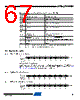
65 / 236 page  65 8006H–AVR–10/09 ATtiny24/44/84 10.2.2 Alternate Functions of Port B The Port B pins with alternate function are shown in Table 10-7. • Port B, Bit 0 – XTAL1/PCINT8 • XTAL1: Chip Clock Oscillator pin 1. Used for all chip clock sources except internal calibrateble RC oscillator. When used as a clock pin, the pin can not be used as an I/O pin. When using internal calibratable RC Oscillator as a chip clock source, PB0 serves as an ordinary I/O pin. •PCINT8: Pin Change Interrupt source 8. The PB0 pin can serve as an external interrupt source for pin change interrupt 1. • CLKI: Clock Input from an external clock source, see “External Clock” on page 26. • Port B, Bit 1 – XTAL2/PCINT9 • XTAL2: Chip Clock Oscillator pin 2. Used as clock pin for all chip clock sources except internal calibrateble RC Oscillator and external clock. When used as a clock pin, the pin can not be used as an I/O pin. When using internal calibratable RC Oscillator or External clock as a Chip clock sources, PB1 serves as an ordinary I/O pin. •PCINT9: Pin Change Interrupt source 9. The PB1 pin can serve as an external interrupt source for pin change interrupt 1. • Port B, Bit 2 – INT0/OC0A/CKOUT/PCINT10 •INT0: External Interrupt Request 0. • OC0A: Output Compare Match output: The PB2 pin can serve as an external output for the Timer/Counter0 Compare Match A. The PB2 pin has to be configured as an output (DDB2 set (one)) to serve this function. The OC0A pin is also the output pin for the PWM mode timer function. • CKOUT - System Clock Output: The system clock can be output on the PB2 pin. The system clock will be output if the CKOUT Fuse is programmed, regardless of the PORTB2 and DDB2 settings. It will also be output during reset. •PCINT10: Pin Change Interrupt source 10. The PB2 pin can serve as an external interrupt source for pin change interrupt 1. Table 10-7. Port B Pins Alternate Functions Port Pin Alternate Function PB0 XTAL1: Crystal Oscillator Input PCINT8: Pin Change Interrupt 1, Source 8 CLKI: External Clock Input PB1 XTAL2: Crystal Oscillator Output PCINT9: Pin Change Interrupt 1, Source 9 PB2 INT0: External Interrupt 0 Input OC0A: Timer/Counter0 Compare Match A output CKOUT: System Clock Output PCINT10:Pin Change Interrupt 1, Source 10 PB3 RESET: Reset pin dW:debugWire I/O PCINT11:Pin Change Interrupt 1, Source 11. |
|
Enlace URL |
| ¿ALLDATASHEET es útil para Ud.? [ DONATE ] |
Todo acerca de Alldatasheet | Publicidad | Contáctenos | Política de Privacidad | Enlace a la hoja de datos | Intercambio de Enlaces | Lista de Fabricantes All Rights Reserved©Alldatasheet.com |
| Russian : Alldatasheetru.com | Korean : Alldatasheet.co.kr | Spanish : Alldatasheet.es | French : Alldatasheet.fr | Italian : Alldatasheetit.com Portuguese : Alldatasheetpt.com | Polish : Alldatasheet.pl | Vietnamese : Alldatasheet.vn Indian : Alldatasheet.in | Mexican : Alldatasheet.com.mx | British : Alldatasheet.co.uk | New Zealand : Alldatasheet.co.nz |
|
Family Site : ic2ic.com |
icmetro.com |
 Spanish ▼
 English
 Chinese
 German
 Japanese
 Russian
 Korean
 Spanish
 French
 Italian
 Portuguese
 Polish
 Vietnamese
 Indian
 Mexican
 British
 New Zealand