|
Motor de Búsqueda de Datasheet de Componentes Electrónicos |
|
|
Motor de Búsqueda de Datasheet de Componentes Electrónicos |
|
AD7715 Datasheet(PDF) 15 Page - Analog Devices |
|
|
|||||||||||||||||||||||||||||
AD7715 Datasheet(HTML) 15 Page - Analog Devices |
|
|
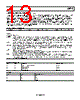
15 / 40 page  AD7715 Rev. D | Page 15 of 40 Table 13. MD1 MD0 Operating Mode 0 0 Normal mode. This operating mode is the default mode of operation of the device whereby the device is performing normal conversions. The AD7705 is placed in this mode after power-on or reset. 0 1 Self-calibration. This is a one step calibration sequence and when complete the part returns to normal mode with MD1 and MD0 returning to 0, 0. The DRDY output or DRDYbit goes high when calibration is initiated and returns low when this self- calibration is complete and a new valid word is available in the data register. The zero-scale calibration is performed at the selected gain on internally shorted (zeroed) inputs and the full-scale calibration is performed at the selected gain on an internally generated VREF/selected gain. 1 0 Zero-scale system calibration. Zero-scale system calibration is performed at the selected gain on the input voltage provided at the analog input during this calibration sequence. This input voltage should remain stable for the duration of the calibration. The DRDY output or DRDY bit goes high when calibration is initiated and returns low when this zero-scale calibration is complete and a new valid word is available in the data register. At the end of the calibration, the part returns to normal mode with MD1 and MD0 returning to 0, 0. 1 1 Full-scale system calibration. Full-scale system calibration is performed at the selected gain on the input voltage provided at the analog input during this calibration sequence. This input voltage should remain stable for the duration of the calibration. The DRDY output or DRDY bit goes high when calibration is initiated and returns low when this full-scale calibration is complete and a new valid word is available in the data register. At the end of the calibration, the part returns to normal mode with MD1 and MD0 returning to 0, 0. Table 14. Output Update Rates CLK1 FS1 FS0 Output Update Rate −3 dB Filter Cutoff 0 0 0 20 Hz 5.24 Hz 0 0 1 25 Hz 6.55 Hz 0 1 0 100 Hz 26.2 Hz 0 1 1 200 Hz 52.4 Hz 1 0 0 50 Hz 13.1 Hz 1 0 1 60 Hz 15.7 Hz (default status) 1 1 0 250 Hz 65.5 Hz 1 1 1 500 Hz 131 Hz 1 Assumes correct clock frequency at MCLK IN pin. TEST REGISTER (RS1, RS0 = 1, 0) The part contains a test register, which is used in testing the device. The user is advised not to change the status of any of the bits in this register from the default (power-on or reset) status of all 0s as the part will be placed in one of its test modes and will not operate correctly. If the part enters one of its test modes, exercising RESET will exit the part from the mode. An alterna- tive scheme for getting the part out of one of its test modes, is to reset the interface by writing 32 successive 1s to the part and then load all 0s to the test register. DATA REGISTER (RS1, RS0 = 1, 1) The data register on the part is a read-only 16-bit register that contains the most up-to-date conversion result from the AD7715. If the communications register data sets up the part for a write operation to this register, a write operation must actually take place to return the part to where it is expecting a write operation to the communications register (the default state of the interface). However, the 16 bits of data written to the part will be ignored by the AD7715. |
|
Enlace URL |
| ¿ALLDATASHEET es útil para Ud.? [ DONATE ] |
Todo acerca de Alldatasheet | Publicidad | Contáctenos | Política de Privacidad | Enlace a la hoja de datos | Intercambio de Enlaces | Lista de Fabricantes All Rights Reserved©Alldatasheet.com |
| Russian : Alldatasheetru.com | Korean : Alldatasheet.co.kr | Spanish : Alldatasheet.es | French : Alldatasheet.fr | Italian : Alldatasheetit.com Portuguese : Alldatasheetpt.com | Polish : Alldatasheet.pl | Vietnamese : Alldatasheet.vn Indian : Alldatasheet.in | Mexican : Alldatasheet.com.mx | British : Alldatasheet.co.uk | New Zealand : Alldatasheet.co.nz |
|
Family Site : ic2ic.com |
icmetro.com |
 Spanish ▼
 English
 Chinese
 German
 Japanese
 Russian
 Korean
 Spanish
 French
 Italian
 Portuguese
 Polish
 Vietnamese
 Indian
 Mexican
 British
 New Zealand