|
Motor de Búsqueda de Datasheet de Componentes Electrónicos |
|
|
Motor de Búsqueda de Datasheet de Componentes Electrónicos |
|
AD7715 Datasheet(PDF) 14 Page - Analog Devices |
|
|
|||||||||||||||||||||||||||||
AD7715 Datasheet(HTML) 14 Page - Analog Devices |
|
|
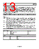
14 / 40 page  AD7715 Rev. D | Page 14 of 40 SETUP REGISTER (RS1, RS0 = 0, 1); POWER ON/RESET STATUS: 28 HEX The setup register is an eight-bit register from which data can either be read or to which data can be written. This register controls the setup that the device is to operate in such as the calibration mode, and output rate, unipolar/bipolar operation etc. Table 11 outlines the bit designations for the setup register. Table 11. Setup Register MD1 MD0 CLK FS1 FS0 B/U BUF FSYNC Table 12. Bit Name Description MD1, MD0 Mode select bits. These bits select the operating mode of the AD7715 (see Table 13). CLK The clock bit (CLK) should be set in accordance with the operating frequency of the AD7715. If the device has a master clock frequency of 2.4576 MHz, then this bit should be set to a 1. If the device has a master clock frequency of 1 MHz, then this bit should be set to a 0. This bit sets up the correct scaling currents for a given master clock and also chooses (along with FS1 and FS0) the output update rate for the device. If this bit is not set correctly for the master clock frequency of the device, then the device may not operate to specification. The default value for this bit after power-on or reset is 1. FS1, FS0 Along with the CLK bit, FS1 and FS0 determine the output update rate, filter first notch and −3 dB frequency as outlined in Table 14. The on-chip digital filter provides a sinc3 (or (Sinx/x)3) filter response. In association with the gain selection, it also determines the output noise (and therefore, the resolution) of the device. Changing the filter notch frequency, as well as the selected gain, impacts resolution. Table 15 through Table 22 show the effect of the filter notch frequency and gain on the output noise and effective resolution of the part. The output data rate (or effective conversion time) for the device is equal to the frequency selected for the first notch of the filter. For example, if the first notch of the filter is selected at 50 Hz then a new word is available at a 50 Hz rate or every 20 ms. If the first notch is at 500 Hz, a new word is available every 2 ms. The default value for these bits is 1, 0. The settling-time of the filter to a full-scale step input change is worst case 4 × 1/(output data rate). For example, with the first filter notch at 50 Hz, the settling time of the filter to a full-scale step input change is 80 ms maximum. If the first notch is at 500 Hz, the settling time of the filter to a full-scale input step is 8 ms max. This settling-time can be reduced to 3 × 1/(output data rate) by synchronizing the step input change to a reset of the digital filter. In other words, if the step input takes place with the FSYNC bit high, the settling-time time is 3 × 1/(output data rate) from when FSYNC returns low. The −3 dB frequency is determined by the programmed first notch frequency according to the relationship: filter −3 dB frequency = 0.262 × filter first notch frequency B/U A 0 in this bipolar/unipolar operation bit selects bipolar operation. This is the default (power-on or reset) status of this bit. A 1 in this bit selects unipolar operation. BUF With this buffer control bit low, the on-chip buffer on the analog input is shorted out. With the buffer shorted out, the current flowing in the AVDD line is reduced to 250 μA (all gains at fCLK IN = 1 MHz and gain of 1 or 2 at fCLK IN = 2.4576 MHz) or 500 μA (gains of 32 and 128 @ fCLK IN = 2.4576 MHz) and the output noise from the part is at its lowest. When this bit is high, the on- chip buffer is in series with the analog input allowing the input to handle higher source impedances. FSYNC When this filter synchronization bit is high, the nodes of the digital filter, the filter control logic and the this bit goes low, the modulator and filter start to process data and a valid word is available in 3 × 1/(output update rate), that is, the settling-time of the filter. This FSYNC bit does not affect the digital interface and does not reset the DRDY output if it is low. |
|
Enlace URL |
| ¿ALLDATASHEET es útil para Ud.? [ DONATE ] |
Todo acerca de Alldatasheet | Publicidad | Contáctenos | Política de Privacidad | Enlace a la hoja de datos | Intercambio de Enlaces | Lista de Fabricantes All Rights Reserved©Alldatasheet.com |
| Russian : Alldatasheetru.com | Korean : Alldatasheet.co.kr | Spanish : Alldatasheet.es | French : Alldatasheet.fr | Italian : Alldatasheetit.com Portuguese : Alldatasheetpt.com | Polish : Alldatasheet.pl | Vietnamese : Alldatasheet.vn Indian : Alldatasheet.in | Mexican : Alldatasheet.com.mx | British : Alldatasheet.co.uk | New Zealand : Alldatasheet.co.nz |
|
Family Site : ic2ic.com |
icmetro.com |
 Spanish ▼
 English
 Chinese
 German
 Japanese
 Russian
 Korean
 Spanish
 French
 Italian
 Portuguese
 Polish
 Vietnamese
 Indian
 Mexican
 British
 New Zealand