|
Motor de Búsqueda de Datasheet de Componentes Electrónicos |
|
|
Motor de Búsqueda de Datasheet de Componentes Electrónicos |
|
AD7715 Datasheet(PDF) 12 Page - Analog Devices |
|
|
|||||||||||||||||||||||||||||
AD7715 Datasheet(HTML) 12 Page - Analog Devices |
|
|
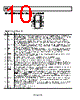
12 / 40 page  AD7715 Rev. D | Page 12 of 40 ON-CHIP REGISTERS The AD7715 contains four on-chip registers, which can be accessed by via the serial port on the part. The first of these is a communications register that decides whether the next operation is a read or write operation and also decides which register the read or write operation accesses. All communi- cations to the part must start with a write operation to the communications register. After power-on or RESET, the device expects a write to its communications register. The data written to this register determines whether the next operation to the part is a write or a read operation and also determines to which register this read or write operation occurs. Therefore, write access to any of the other registers on the part starts with a write operation to the communications register followed by a write to the selected register. A read operation from any register on the part (including the communications register itself and the output data register) starts with a write operation to the communications register followed by a read operation from the selected register. The communication register also controls the standby mode and the operating gain of the part. The DRDY status is also available by reading from the communications register. The second register is a setup register that determines calibration modes, filter selection and bipolar/unipolar operation. The third register is the data register from which the output data from the part is accessed. The final register is a test register that is accessed when testing the device. It is advised that the user does not attempt to access or change the contents of the test register as it may lead to unspecified operation of the device. The registers are discussed in more detail in the following sections. |
|
Enlace URL |
| ¿ALLDATASHEET es útil para Ud.? [ DONATE ] |
Todo acerca de Alldatasheet | Publicidad | Contáctenos | Política de Privacidad | Enlace a la hoja de datos | Intercambio de Enlaces | Lista de Fabricantes All Rights Reserved©Alldatasheet.com |
| Russian : Alldatasheetru.com | Korean : Alldatasheet.co.kr | Spanish : Alldatasheet.es | French : Alldatasheet.fr | Italian : Alldatasheetit.com Portuguese : Alldatasheetpt.com | Polish : Alldatasheet.pl | Vietnamese : Alldatasheet.vn Indian : Alldatasheet.in | Mexican : Alldatasheet.com.mx | British : Alldatasheet.co.uk | New Zealand : Alldatasheet.co.nz |
|
Family Site : ic2ic.com |
icmetro.com |
 Spanish ▼
 English
 Chinese
 German
 Japanese
 Russian
 Korean
 Spanish
 French
 Italian
 Portuguese
 Polish
 Vietnamese
 Indian
 Mexican
 British
 New Zealand