 |
Motor de Búsqueda de Datasheet de Componentes Electrónicos |
|
|
Motor de Búsqueda de Datasheet de Componentes Electrónicos |
|
The question interval is too short.
Please try again in a few seconds.

Hello, Please ask a question about AD7715_15 Datasheet
# Example questions:
➢ What is the maximum absolute voltage allowed on the ain/ref in pins?
➢ How does the buf bit in the setup register affect the ain input?
➢ What is the typical input common-mode rejection (cmr) of the ad7715?
| Part No. | AD7715_15 |
| Manufacturer | AD |
| Size | 495 Kbytes |
| Pages | 40 pages |
| Description | 16-Bit, Sigma-Delta ADC |

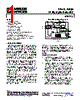
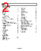
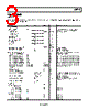
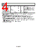
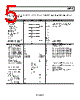
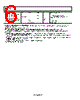
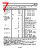
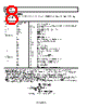
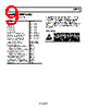
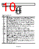
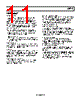
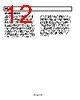
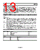
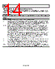


Okay, let's break down the information provided in these two tables about the AD7715. Here's a consolidated summary, focusing on key parameters and differences between the "A" version and the "AD" version.
Overall Context
️· AD7715: This is an ADC (Analog-to-Digital Converter) device.
️· Two Versions: There are two versions presented:
- "A" Version: Designed for a supply voltage of 3.3V.
- "AD" Version: Designed for a supply voltage of 1.8V.
Key Parameter Comparison
| Feature | "A" Version (3.3V Supply) | "AD" Version (1.8V Supply) |
|---|---|---|
| Supply Voltage | 3.3V | 1.8V |
| Input Range | 0 to +VREF/GAIN (typically 3.3V) | 0 to +VREF/GAIN (typically 1.8V) |
| Reference Voltage (VREF) | Typically 3.3V | Typically 1.8V |
| Input Sampling Rate (fS) | GAIN x fCLK / 64 | GAIN x fCLK / 64 |
| Differential Input Range | Up to 1.5V | Up to 1.5V |
| Input Current (Logic Inputs) | ±10μA | ±10μA |
| Output Low Voltage (VOL) | 0.4V | 0.4V |
| Output High Voltage (VOH) | DVDD - 0.6V | DVDD - 0.6V |
| Common Mode Rejection (CMR) | 90 dB | 90 dB |
| Input Offset & Gain Error | +/- 0.0015 | Typically +/- 0.0004% |
| Full Scale Drift | 0.2 μV/°C | 0.2 μV/°C |
| Gain Drift | 0.2 μV/°C | 0.2 μV/°C|
Important Notes & Other Details
️· Reference Voltage: The reference voltage directly impacts the input range.
️· GAIN: The "GAIN" parameter appears in various calculations related to sampling rate and input range. It likely refers to an internal amplifier gain setting.
️· fCLK: This is the clock frequency, which determines the overall sampling rate.
️· Digital Output Coding: Both versions support Binary and Offset Binary digital output coding.
️· Logic Inputs: The logic input current is the same in both versions.
️· Temperature Sensitivity: Both versions have similar temperature sensitivities.
In short: The main difference between the "A" and "AD" versions is the supply voltage, which affects the input range. The other electrical characteristics are very similar.
Overall Context
️· AD7715: This is an ADC (Analog-to-Digital Converter) device.
️· Two Versions: There are two versions presented:
- "A" Version: Designed for a supply voltage of 3.3V.
- "AD" Version: Designed for a supply voltage of 1.8V.
Key Parameter Comparison
| Feature | "A" Version (3.3V Supply) | "AD" Version (1.8V Supply) |
|---|---|---|
| Supply Voltage | 3.3V | 1.8V |
| Input Range | 0 to +VREF/GAIN (typically 3.3V) | 0 to +VREF/GAIN (typically 1.8V) |
| Reference Voltage (VREF) | Typically 3.3V | Typically 1.8V |
| Input Sampling Rate (fS) | GAIN x fCLK / 64 | GAIN x fCLK / 64 |
| Differential Input Range | Up to 1.5V | Up to 1.5V |
| Input Current (Logic Inputs) | ±10μA | ±10μA |
| Output Low Voltage (VOL) | 0.4V | 0.4V |
| Output High Voltage (VOH) | DVDD - 0.6V | DVDD - 0.6V |
| Common Mode Rejection (CMR) | 90 dB | 90 dB |
| Input Offset & Gain Error | +/- 0.0015 | Typically +/- 0.0004% |
| Full Scale Drift | 0.2 μV/°C | 0.2 μV/°C |
| Gain Drift | 0.2 μV/°C | 0.2 μV/°C |
| Part No. | AD7715_15 |
| Manufacturer | AD |
| Size | 495 Kbytes |
| Pages | 40 pages |
| Description | 16-Bit, Sigma-Delta ADC |
| ¿ALLDATASHEET es útil para Ud.? [ DONATE ] |
Todo acerca de Alldatasheet | Publicidad | Contáctenos | Política de Privacidad | Enlace a la hoja de datos | Intercambio de Enlaces | Lista de Fabricantes All Rights Reserved©Alldatasheet.com |
| Russian : Alldatasheetru.com | Korean : Alldatasheet.co.kr | Spanish : Alldatasheet.es | French : Alldatasheet.fr | Italian : Alldatasheetit.com Portuguese : Alldatasheetpt.com | Polish : Alldatasheet.pl | Vietnamese : Alldatasheet.vn Indian : Alldatasheet.in | Mexican : Alldatasheet.com.mx | British : Alldatasheet.co.uk | New Zealand : Alldatasheet.co.nz |
|
Family Site : ic2ic.com |
icmetro.com |
 Spanish ▼
  English
 Chinese
 German
 Japanese
 Russian
 Korean
 French
 Italian
 Portuguese
 Polish
 Vietnamese
 Indian
 Mexican
 British
 New Zealand