|
Motor de Búsqueda de Datasheet de Componentes Electrónicos |
|
|
Motor de Búsqueda de Datasheet de Componentes Electrónicos |
|
CC1150-RTR1 Datasheet(PDF) 15 Page - Texas Instruments |
|
|
|||||||||||||||||||||||||||||
CC1150-RTR1 Datasheet(HTML) 15 Page - Texas Instruments |
|
|
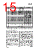
15 / 67 page  CC1150 SWRS037A Page 15 of 60 Component Value at 31 5MHz Value at 433 MHz Value at 868/915 MHz C41 100 nF ± 10%, 0402 X5R C51 27 pF ± 5%, 0402 NP0 C71 27 pF ± 5%, 0402 NP0 C101 6.8 pF ± 0.5 pF, 0402 NP0 3.9 pF ± 0.25 pF, 0402 NP0 1.0 pF ± 0.25 pF, 0402 NP0 C102 12 pF ± 5%, 0402 NP0 8.2 pF ± 0.5 pF, 0402 NP0 1.5 pF ± 0.25 pF, 0402 NP0 C103 6.8 pF ± 0.5 pF, 0402 NP0 5.6pF±0.5pF, 0402 NP0 3.3 pF ± 0.25 pF, 0402 NP0 C104 220 pF ± 5%, 0402 NP0 220 pF ± 5%, 0402 NP0 100 pF ± 5%, 0402 NP0 C105 220 pF ± 5%, 0402 NP0 220 pF ± 5%, 0402 NP0 100 pF ± 5%, 0402 NP0 (12 pF ± 5%, 0402 NP0 if optionally 699 MHz filter is desired) C106 (47 pF ± 5%, 0402 NP0 if optionally 699 MHz filter is desired) C111 6.8 pF ± 0.5 pF, 0402 NP0 3.9 pF ± 0.25 pF, 0402 NP0 1.5 pF ± 0.25pF, 0402 NP0 L101 33nH±5%, 0402 monolithic 27 nH ± 5%, 0402 monolithic 12 nH ± 5%, 0402 monolithic L102 18nH±5%, 0402 monolithic 22 nH ± 5%, 0402 monolithic 18 nH ± 5%, 0402 monolithic L103 33 nH ± 5%, 0402 monolithic 27 nH ± 5%, 0402 monolithic 12 nH ± 5%, 0402 monolithic L104 (12 nH ± 5%, 0402 monolithic if optionally 699 MHz filter is desired) L105 3.3 nH ± 5%, 0402 monolithic L111 33 nH ± 5%, 0402 monolithic 27 nH ± 5%, 0402 monolithic 12 nH ± 5%, 0402 monolithic L112 18 nH ± 5%, 0402 monolithic R141 56 kΩ±1%, 0402 XTAL 26.0 MHz surface mount crystal Table 14: Bill of Materials for the Application Circuit (Murata LQG15HS and GRM1555C series inductors and capacitors, resistor from the Koa RK73 series, and AT-41CD2 crystal from NDK) 7.8 PCB Layout Recommendations The top layer should be used for signal routing, and the open areas should be filled with metallization connected to ground using several vias. The area under the chip is used for grounding and shall be connected to the bottom ground plane with several vias for good thermal performance and sufficiently low inductance to ground. In the CC1150EM reference designs ([1] and [2]), 5 vias are placed inside the exposed die attached pad. These vias should be “tented” (covered with solder mask) on the component side of the PCB to avoid migration of solder through the vias during the solder reflow process. The solder paste coverage should not be 100%. If it is, out gassing may occur during the reflow process, which may cause defects (splattering, solder balling). Using “tented” vias reduces the solder paste coverage below 100%. See Figure 6 for top solder resist and top paste masks. All the decoupling capacitors should be placed as close as possible to the supply pin it is supposed to decouple. Each decoupling capacitor should be connected to the power line (or power plane) by separate vias. The best routing is from the power line (or power plane) to the decoupling capacitor and then to the CC1150 supply pin. Supply power filtering is very important. Each decoupling capacitor ground pad should be connected to the ground plane by separate vias. Direct connections between neighboring power pins will increase noise coupling and should be avoided unless absolutely necessary. Routing in the ground plane underneath and between the chip, the balun/RF matching circuit and the decoupling capacitor’s ground vias should also be |
|
Enlace URL |
| ¿ALLDATASHEET es útil para Ud.? [ DONATE ] |
Todo acerca de Alldatasheet | Publicidad | Contáctenos | Política de Privacidad | Enlace a la hoja de datos | Intercambio de Enlaces | Lista de Fabricantes All Rights Reserved©Alldatasheet.com |
| Russian : Alldatasheetru.com | Korean : Alldatasheet.co.kr | Spanish : Alldatasheet.es | French : Alldatasheet.fr | Italian : Alldatasheetit.com Portuguese : Alldatasheetpt.com | Polish : Alldatasheet.pl | Vietnamese : Alldatasheet.vn Indian : Alldatasheet.in | Mexican : Alldatasheet.com.mx | British : Alldatasheet.co.uk | New Zealand : Alldatasheet.co.nz |
|
Family Site : ic2ic.com |
icmetro.com |
 Spanish ▼
 English
 Chinese
 German
 Japanese
 Russian
 Korean
 Spanish
 French
 Italian
 Portuguese
 Polish
 Vietnamese
 Indian
 Mexican
 British
 New Zealand