|
Motor de Búsqueda de Datasheet de Componentes Electrónicos |
|
|
Motor de Búsqueda de Datasheet de Componentes Electrónicos |
|
CC1150-RTR1 Datasheet(PDF) 38 Page - Texas Instruments |
|
|
|||||||||||||||||||||||||||||
CC1150-RTR1 Datasheet(HTML) 38 Page - Texas Instruments |
|
|
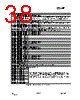
38 / 67 page  CC1150 SWRS037A Page 38 of 60 GDOx_CFG[5:0] Description 0 (0x00) Reserved – defined on the transceiver version ( CC1101). 1 (0x01) Reserved – defined on the transceiver version ( CC1101). 2 (0x02) Associated to the TX FIFO: Asserts when the TX FIFO is filled at or above the TX FIFO threshold. De-asserts when the TX FIFO is below the same threshold. 3 (0x03) Associated to the TX FIFO: Asserts when TX FIFO is full. De-asserts when the TX FIFO is drained below the TX FIFO threshold. 4 (0x04) Reserved – defined on the transceiver version ( CC1101). 5 (0x05) Asserts when the TX FIFO has underflowed. De-asserts when the FIFO is flushed. 6 (0x06) Asserts when sync word has been sent, and de-asserts at the end of the packet. In TX the pin will also de-assert if the TX FIFO underflows. 7 (0x07) Reserved – defined on the transceiver version ( CC1101). 8 (0x08) Reserved – defined on the transceiver version ( CC1101). 9 (0x09) Reserved – defined on the transceiver version ( CC1101). 10 (0x0A) Lock detector output. The PLL is in lock if the lock detector output has a positive transition or is constantly logic high. To check for PLL lock the lock detector output should be used as an interrupt for the MCU. 11 (0x0B) Serial Clock. Synchronous to the data in synchronous serial mode. In TX mode, data is sampled by CC1150 on the rising edge of the serial clock when GDOx_INV=0. 12 (0x0C) Reserved – defined on the transceiver version ( CC1101). 13 (0x0D) Reserved – defined on the transceiver version ( CC1101). 14 (0x0E) Reserved – defined on the transceiver version ( CC1101). 15 (0x0F) Reserved – defined on the transceiver version ( CC1101). 16 (0x10) Reserved – used for test. 17 (0x11) Reserved – used for test. 18 (0x12) Reserved – used for test. 19 (0x13) Reserved – used for test. 20 (0x14) Reserved – used for test. 21 (0x15) Reserved – used for test. 22 (0x16) Reserved – defined on the transceiver version ( CC1101). 23 (0x17) Reserved – defined on the transceiver version ( CC1101). 24 (0x18) Reserved – used for test. 25 (0x19) Reserved – used for test. 26 (0x1A) Reserved – used for test. 27 (0x1B) PA_PD. PA is enabled when 1, in power-down when 0. 28 (0x1C) Reserved – defined on the transceiver version ( CC1101). 29 (0x1D) Reserved – defined on the transceiver version ( CC1101). 30 (0x1E) Reserved – used for test. 31 (0x1F) Reserved – used for test. 32 (0x20) Reserved – used for test. 33 (0x21) Reserved – used for test. 34 (0x22) Reserved – used for test. 35 (0x23) Reserved – used for test. 36 (0x24) Reserved – defined on the transceiver version ( CC1101). 37 (0x25) Reserved – defined on the transceiver version ( CC1101). 38 (0x26) Reserved – used for test. 39 (0x27) Reserved – defined on the transceiver version ( CC1101). 40 (0x28) Reserved – used for test. 41 (0x29) CHIP_RDYn. 42 (0x2A) Reserved – used for test. 43 (0x2B) XOSC_STABLE. 44 (0x2C) Reserved – used for test. 45 (0x2D) GDO0 _Z_EN_N. When this output is 0, GDO0 is configured as input (for serial TX data). 46 (0x2E) High impedance (3-state). 47 (0x2F) HW to 0 (HW1 achieved by setting GDOx_INV=1). 48 (0x30) CLK_XOSC/1 49 (0x31) CLK_XOSC/1.5 50 (0x32) CLK_XOSC/2 51 (0x33) CLK_XOSC/3 52 (0x34) CLK_XOSC/4 53 (0x35) CLK_XOSC/6 54 (0x36) CLK_XOSC/8 55 (0x37) CLK_XOSC/12 56 (0x38) CLK_XOSC/16 57 (0x39) CLK_XOSC/24 58 (0x3A) CLK_XOSC/32 59 (0x3B) CLK_XOSC/48 60 (0x3C) CLK_XOSC/64 61 (0x3D) CLK_XOSC/96 62 (0x3E) CLK_XOSC/128 63 (0x3F) CLK_XOSC/192 Note: There are 2 GDO pins, but only one CLK_XOSC/n can be selected as an output at any time. If CLK_XOSC/n is to be monitored on one of the GDO pins, the other GDO pin must be configured to values less than 0x30. The GDO0 default value is CLK_XOSC/192. To optimize RF performance, these signals should not be used while the radio is in TX mode. Table 24: GDO signal selection(x = 0 or 1) |
|
Enlace URL |
| ¿ALLDATASHEET es útil para Ud.? [ DONATE ] |
Todo acerca de Alldatasheet | Publicidad | Contáctenos | Política de Privacidad | Enlace a la hoja de datos | Intercambio de Enlaces | Lista de Fabricantes All Rights Reserved©Alldatasheet.com |
| Russian : Alldatasheetru.com | Korean : Alldatasheet.co.kr | Spanish : Alldatasheet.es | French : Alldatasheet.fr | Italian : Alldatasheetit.com Portuguese : Alldatasheetpt.com | Polish : Alldatasheet.pl | Vietnamese : Alldatasheet.vn Indian : Alldatasheet.in | Mexican : Alldatasheet.com.mx | British : Alldatasheet.co.uk | New Zealand : Alldatasheet.co.nz |
|
Family Site : ic2ic.com |
icmetro.com |
 Spanish ▼
 English
 Chinese
 German
 Japanese
 Russian
 Korean
 Spanish
 French
 Italian
 Portuguese
 Polish
 Vietnamese
 Indian
 Mexican
 British
 New Zealand