|
Motor de Búsqueda de Datasheet de Componentes Electrónicos |
|
|
Motor de Búsqueda de Datasheet de Componentes Electrónicos |
|
M29DW128F60NF1F Datasheet(PDF) 15 Page - STMicroelectronics |
|
|
|||||||||||||||||||||||||||||
M29DW128F60NF1F Datasheet(HTML) 15 Page - STMicroelectronics |
|
|
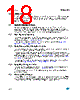
15 / 93 page  M29DW128F 2 Signal descriptions 15/93 2.7 Write Enable (W) The Write Enable pin, W, controls the Bus Write operation of the memory’s Command Interface. 2.8 VPP/Write Protect (VPP/WP) The VPP/Write Protect pin provides two functions. The VPP function allows the memory to use an external high voltage power supply to reduce the time required for Program operations. This is achieved by bypassing the unlock cycles and/or using the multiple Word (2 or 4 at-a-time) or multiple Byte Program (2, 4 or 8 at-a-time) commands. The Write Protect function provides a hardware method of protecting the four outermost boot blocks (two at the top, and two at the bottom of the address space). When VPP/Write Protect is Low, VIL, the memory protects the four outermost boot blocks; Program and Erase operations in these blocks are ignored while VPP/Write Protect is Low, even when RP is at VID. When VPP/Write Protect is High, VIH, the memory reverts to the previous protection status of the four outermost boot blocks. Program and Erase operations can now modify the data in these blocks unless the blocks are protected using Block Protection. Applying VPPH to the VPP/WP pin will temporarily unprotect any block previously protected (including the four outermost parameter blocks) using a High Voltage Block Protection technique (In-System or Programmer technique). See Table 9: Hardware Protection for details. When VPP/Write Protect is raised to VPP the memory automatically enters the Unlock Bypass mode. When VPP/Write Protect returns to VIH or VIL normal operation resumes. During Unlock Bypass Program operations the memory draws IPP from the pin to supply the programming circuits. See the description of the Unlock Bypass command in the Command Interface section. The transitions from VIH to VPP and from VPP to VIH must be slower than tVHVPP, see Figure 20. Never raise VPP/Write Protect to VPP from any mode except Read mode, otherwise the memory may be left in an indeterminate state. The VPP/Write Protect pin must not be left floating or unconnected or the device may become unreliable. A 0.1µF capacitor should be connected between the VPP/Write Protect pin and the VSS Ground pin to decouple the current surges from the power supply. The PCB track widths must be sufficient to carry the currents required during Unlock Bypass Program, IPP. 2.9 Reset/Block Temporary Unprotect (RP) The Reset/Block Temporary Unprotect pin can be used to apply a Hardware Reset to the memory or to temporarily unprotect all the blocks previously protected using a High Voltage Block Protection technique (In-System or Programmer technique). Note that if VPP/WP is at VIL, then the four outermost parameter blocks will remain protected even if RP is at VID. A Hardware Reset is achieved by holding Reset/Block Temporary Unprotect Low, VIL, for at least tPLPX. After Reset/Block Temporary Unprotect goes High, VIH, the memory will be ready for Bus Read and Bus Write operations after tPHEL or tRHEL, whichever occurs last. See the Ready/Busy Output section, Table 30: Reset/Block Temporary Unprotect AC Characteristics and Figure 18 and Figure 19 for more details. |
|
Enlace URL |
| ¿ALLDATASHEET es útil para Ud.? [ DONATE ] |
Todo acerca de Alldatasheet | Publicidad | Contáctenos | Política de Privacidad | Enlace a la hoja de datos | Intercambio de Enlaces | Lista de Fabricantes All Rights Reserved©Alldatasheet.com |
| Russian : Alldatasheetru.com | Korean : Alldatasheet.co.kr | Spanish : Alldatasheet.es | French : Alldatasheet.fr | Italian : Alldatasheetit.com Portuguese : Alldatasheetpt.com | Polish : Alldatasheet.pl | Vietnamese : Alldatasheet.vn Indian : Alldatasheet.in | Mexican : Alldatasheet.com.mx | British : Alldatasheet.co.uk | New Zealand : Alldatasheet.co.nz |
|
Family Site : ic2ic.com |
icmetro.com |
 Spanish ▼
 English
 Chinese
 German
 Japanese
 Russian
 Korean
 Spanish
 French
 Italian
 Portuguese
 Polish
 Vietnamese
 Indian
 Mexican
 British
 New Zealand