|
Motor de Búsqueda de Datasheet de Componentes Electrónicos |
|
|
Motor de Búsqueda de Datasheet de Componentes Electrónicos |
|
MC7660 Datasheet(PDF) 5 Page - ON Semiconductor |
|
|
|||||||||||||||||||||||||||||
MC7660 Datasheet(HTML) 5 Page - ON Semiconductor |
|
|
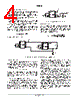
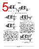
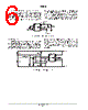
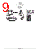
5 / 12 page  MC7660 http://onsemi.com 5 Figure 5. Increased Output Voltage by Cascading Devices MC7660 1 2 3 4 8 7 6 5 V+ MC7660 1 2 3 4 8 7 6 5 + 10 mF + 10 mF 10 mF + VOUT* *NOTE: VOUT = –n V+ for 1.5 V ≤ V+ ≤ 10 V “1” “n” Figure 6. External Clocking MC7660 1 2 3 4 8 7 6 5 V+ + + 10 mF VOUT V+ 1 k W CMOS GATE 10 mF Figure 7. Lowering Oscillator Frequency MC7660 1 2 3 4 8 7 6 5 V+ C1 + + C2 VOUT COSC Positive Voltage Multiplication The MC7660 may be employed to achieve positive voltage multiplication using the circuit shown in Figure 8. In this application, the pump inverter switches of the MC7660 are used to charge C1 to a voltage level of V+ – VF (where V+ is the supply voltage and VF is the forward voltage drop of diode D1). On the transfer cycle, the voltage on C1 plus the supply voltage (V+) is applied through diode D2 to capacitor C2. The voltage thus created on C2 becomes (2 V+) – (2 VF), or twice the supply voltage minus the combined forward voltage drops of diodes D1 and D2. The source impedance of the output (VOUT) will depend on the output current, but for V+ = 5V and an output current of 10 mA, it will be approximately 60 W. Figure 8. Positive Voltage Multiplier MC7660 1 2 3 4 8 7 6 5 V+ + C2 VOUT = (2 V+) – (2 VF) D1 C1 D2 + Combined Negative Voltage Conversion and Positive Supply Multiplication Figure 9 combines the functions shown in Figures 3 and 8 to provide negative voltage conversion and positive voltage multiplication simultaneously. This approach would be, for example, suitable for generating +9V and –5V from an existing +5V supply. In this instance, capacitors C1 and C3 perform the pump and reservoir functions, respectively, for the generation of the negative voltage, while capacitors C2 and C4 are pump and reservoir, respectively, for the multiplied positive voltage. There is a penalty in this configuration which combines both functions, however, in that the source impedances of the generated supplies will be somewhat higher due to the finite impedance of the common charge pump driver at pin 2 of the device. Figure 9. Combined Negative Converter and Positive Muliplier MC7660 1 2 3 4 8 7 6 5 V+ + C4 VOUT = –(V+ – VF) D1 D2 + C3 VOUT = (2 V+) – (2 VF) + C2 + C1 |
|
|
Enlace URL |
| ¿ALLDATASHEET es útil para Ud.? [ DONATE ] |
Todo acerca de Alldatasheet | Publicidad | Contáctenos | Política de Privacidad | Enlace a la hoja de datos | Intercambio de Enlaces | Lista de Fabricantes All Rights Reserved©Alldatasheet.com |
| Russian : Alldatasheetru.com | Korean : Alldatasheet.co.kr | Spanish : Alldatasheet.es | French : Alldatasheet.fr | Italian : Alldatasheetit.com Portuguese : Alldatasheetpt.com | Polish : Alldatasheet.pl | Vietnamese : Alldatasheet.vn Indian : Alldatasheet.in | Mexican : Alldatasheet.com.mx | British : Alldatasheet.co.uk | New Zealand : Alldatasheet.co.nz |
|
Family Site : ic2ic.com |
icmetro.com |
 Spanish ▼
 English
 Chinese
 German
 Japanese
 Russian
 Korean
 Spanish
 French
 Italian
 Portuguese
 Polish
 Vietnamese
 Indian
 Mexican
 British
 New Zealand