|
Motor de Búsqueda de Datasheet de Componentes Electrónicos |
|
|
Motor de Búsqueda de Datasheet de Componentes Electrónicos |
|
MC7660 Datasheet(PDF) 4 Page - ON Semiconductor |
|
|
|||||||||||||||||||||||||||||
MC7660 Datasheet(HTML) 4 Page - ON Semiconductor |
|
|
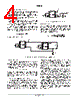
4 / 12 page  MC7660 http://onsemi.com 4 Simple Negative Voltage Converter Figure 3 shows typical connections to provide a negative supply where a positive supply is available. A similar scheme may be employed for supply voltages anywhere in the operating range of +1.5V to +10V, keeping in mind that pin 6 (LV) is tied to the supply negative (GND) only for supply voltages below 3.5V. The output characteristics of the circuit in Figure 3 are those of a nearly ideal voltage source in series with 70 W. Thus, for a load current of –10mA and a supply voltage of +5V, the output voltage would be –4.3V. The dynamic output impedance of the MC7660 is due, primarily, to capacitive reactance of the charge transfer capacitor (C1). Since this capacitor is connected to the output for only 1/2 of the cycle, the equation is: X C + 2 2 pfC 1 + 3.18W, where f = 10kHz and C1 = 10 µF. Figure 3. Simple Negative Converter MC7660 1 2 3 4 8 7 6 5 + + V+ C1 10 mF C2 10 mF VOUT Parallel Devices Any number of MC7660 voltage converters may be paralleled to reduce output resistance (Figure 4). The reservoir capacitor, C2, serves all devices, while each device requires its own pump capacitor, C1. The resultant output resistance would be approximately: R OUT + R OUT (of MC7660) n (number of devices) Figure 4. Paralleling Devices Lowers Output Impedance MC7660 1 2 3 4 8 7 6 5 V+ C1 MC7660 1 2 3 4 8 7 6 5 + C1 C2 RL Cascading Devices The MC7660 may be cascaded as shown (Figure 5) to produce larger negative multiplication of the initial supply voltage. However, due to the finite efficiency of each device, the practical limit is 10 devices for light loads. The output voltage is defined by: VOUT = –n (VIN) where n is an integer representing the number of devices cascaded. The resulting output resistance would be approximately the weighted sum of the individual MC7660 ROUT values. Changing the MC7660 Oscillator Frequency It may be desirable in some applications (due to noise or other considerations) to increase the oscillator frequency. This is achieved by overdriving the oscillator from an external clock, as shown in Figure 6. In order to prevent possible device latch–up, a 1k W resistor must be used in series with the clock output. In a situation where the designer has generated the external clock frequency using TTL logic, the addition of a 10k W pull–up resistor to V+ supply is required. Note that the pump frequency with external clocking, as with internal clocking, will be 1/2 of the clock frequency. Output transitions occur on the positive–going edge of the clock. It is also possible to increase the conversion efficiency of the MC7660 at low load levels by lowering the oscillator frequency. This reduces the switching losses, and is achieved by connecting an additional capacitor, COSC, as shown in Figure 7. Lowering the oscillator frequency will cause an undesirable increase in the impedance of the pump (C1) and the reservoir (C2) capacitors. To overcome this, increase the values of C1 and C2 by the same factor that the frequency has been reduced. For example, the addition of a 100pF capacitor between pin 7 (OSC) and pin 8 (V+) will lower the oscillator frequency to 1kHz from its nominal frequency of 10kHz (a multiple of 10), and necessitate a corresponding increase in the values of C1 and C2 (from 10 µF to 100µF). |
|
|
Enlace URL |
| ¿ALLDATASHEET es útil para Ud.? [ DONATE ] |
Todo acerca de Alldatasheet | Publicidad | Contáctenos | Política de Privacidad | Enlace a la hoja de datos | Intercambio de Enlaces | Lista de Fabricantes All Rights Reserved©Alldatasheet.com |
| Russian : Alldatasheetru.com | Korean : Alldatasheet.co.kr | Spanish : Alldatasheet.es | French : Alldatasheet.fr | Italian : Alldatasheetit.com Portuguese : Alldatasheetpt.com | Polish : Alldatasheet.pl | Vietnamese : Alldatasheet.vn Indian : Alldatasheet.in | Mexican : Alldatasheet.com.mx | British : Alldatasheet.co.uk | New Zealand : Alldatasheet.co.nz |
|
Family Site : ic2ic.com |
icmetro.com |
 Spanish ▼
 English
 Chinese
 German
 Japanese
 Russian
 Korean
 Spanish
 French
 Italian
 Portuguese
 Polish
 Vietnamese
 Indian
 Mexican
 British
 New Zealand