|
Motor de Búsqueda de Datasheet de Componentes Electrónicos |
|
|
Motor de Búsqueda de Datasheet de Componentes Electrónicos |
|
MC7660 Datasheet(PDF) 3 Page - ON Semiconductor |
|
|
|||||||||||||||||||||||||||||
MC7660 Datasheet(HTML) 3 Page - ON Semiconductor |
|
|
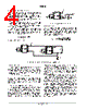
3 / 12 page  MC7660 http://onsemi.com 3 APPLICATIONS INFORMATION Detailed Description The MC7660 contains all the necessary circuitry to implement a voltage inverter, with the exception of two external capacitors, which may be inexpensive 10 µF polarized electrolytic capacitors. Operation is best understood by considering Figure 2, which shows an idealized voltage inverter. Capacitor C1 is charged to a voltage, V+, for the half cycle when switches S1 and S3 are closed. (Note: Switches S2 and S4 are open during this half cycle.) During the second half cycle of operation, switches S2 and S4 are closed, with S1 and S3 open, thereby shifting capacitor C1 negatively by V+ volts. Charge is then transferred from C1 to C2, such that the voltage on C2 is exactly V+, assuming ideal switches and no load on C2. V+ VOUT = –VIN GND S1 S2 S3 S4 C2 Figure 2. Idealized Charge Pump Inverter C1 The four switches in Figure 2 are MOS power switches; S1 is a P–channel device, and S2, S3 and S4 are N–channel devices. The main difficulty with this approach is that in integrating the switches, the substrates of S3 and S4 must always remain reverse–biased with respect to their sources, but not so much as to degrade their ON resistances. In addition, at circuit start–up, and under output short circuit conditions (VOUT = V+), the output voltage must be sensed and the substrate bias adjusted accordingly. Failure to accomplish this will result in high power losses and probable device latch–up. This problem is eliminated in the MC7660 by a logic network which senses the output voltage (VOUT) together with the level translators, and switches the substrates of S3 and S4 to the correct level to maintain necessary reverse bias. The voltage regulator portion of the MC7660 is an integral part of the anti–latch–up circuitry. Its inherent voltage drop can, however, degrade operation at low voltages. To improve low–voltage operation, the LV pin should be connected to GND, disabling the regulator. For supply voltages greater than 3.5V, the LV terminal must be left open to ensure latch–up–proof operation and prevent device damage. Theoretical Power Efficiency Considerations In theory, a capacitive charge pump can approach 100% efficiency if certain conditions are met: (1) The drive circuitry consumes minimal power. (2) The output switches have extremely low ON resistance and virtually no offset. (3) The impedances of the pump and reservoir capacitors are negligible at the pump frequency. The MC7660 approaches these conditions for negative voltage multiplication if large values of C1 and C2 are used. Energy is lost only in the transfer of charge between capacitors if a change in voltage occurs. The energy lost is defined by: E = 1/2 C1 (V12 — V22) V1 and V2 are the voltages on C1 during the pump and transfer cycles. If the impedances of C1 and C2 are relatively high at the pump frequency (refer to Figure 2), compared to the value of RL, there will be a substantial difference in voltages V1 and V2. Therefore, it is not only desirable to make C2 as large as possible to eliminate output voltage ripple, but also to employ a correspondingly large value for C1 in order to achieve maximum efficiency of operation. Dos and Don’ts • Do not exceed maximum supply voltages. • Do not connect LV terminal to GND for supply voltages greater than 3.5V. • Do not short circuit the output to V+ supply for voltages above 5.5V for extended periods; however, transient conditions including start–up are okay. • When using polarized capacitors in the inverting mode, the + terminal of C1 must be connected to pin 2 of the MC7660 and the + terminal of C2 must be connected to GND Pin 3. |
|
|
Enlace URL |
| ¿ALLDATASHEET es útil para Ud.? [ DONATE ] |
Todo acerca de Alldatasheet | Publicidad | Contáctenos | Política de Privacidad | Enlace a la hoja de datos | Intercambio de Enlaces | Lista de Fabricantes All Rights Reserved©Alldatasheet.com |
| Russian : Alldatasheetru.com | Korean : Alldatasheet.co.kr | Spanish : Alldatasheet.es | French : Alldatasheet.fr | Italian : Alldatasheetit.com Portuguese : Alldatasheetpt.com | Polish : Alldatasheet.pl | Vietnamese : Alldatasheet.vn Indian : Alldatasheet.in | Mexican : Alldatasheet.com.mx | British : Alldatasheet.co.uk | New Zealand : Alldatasheet.co.nz |
|
Family Site : ic2ic.com |
icmetro.com |
 Spanish ▼
 English
 Chinese
 German
 Japanese
 Russian
 Korean
 Spanish
 French
 Italian
 Portuguese
 Polish
 Vietnamese
 Indian
 Mexican
 British
 New Zealand