 |
Motor de Búsqueda de Datasheet de Componentes Electrónicos |
|
|
Motor de Búsqueda de Datasheet de Componentes Electrónicos |
|
The question interval is too short.
Please try again in a few seconds.

Hello, Please ask a question about MC7660 Datasheet
# Example questions:
➢ What is the purpose of dimension 'e' in the 8-pin soic package dimensions?
➢ What component is directly manipulated to achieve this adjustment?
➢ How does increasing the load current generally affect the output voltage?
| Part No. | MC7660 |
| Manufacturer | ONSEMI |
| Size | 191 Kbytes |
| Pages | 12 pages |
| Description | Charge Pump DC-to-DC Voltage Converter |



1. Overview - What is the MC7660?
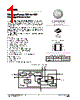
The MC7660 is a monolithic charge pump voltage regulator. In simpler terms, it's an integrated circuit (IC) that generates a higher voltage from a lower input voltage using a technique called charge pumping. This is useful for applications where a higher voltage is needed than what's readily available.
2. Key Features and Applications
️· Charge Pump Architecture: It utilizes a charge pump design, meaning it doesn't rely on a transformer to increase voltage.
️· Adjustable Output Voltage: It's designed to generate a higher voltage, which can be adjusted.
️· Applications: The document highlights it's suitable for a variety of applications, including:
- Non-volatile memory (EEPROM, Flash) programming
- LCD bias
- Set-top box power
- White LED Drivers
- Positive voltage generation
️· Versatility: It seems to be adaptable to different operating conditions and requirements.
3. Technical Specifications & Characteristics (based on figures & text)
️· Input Voltage Range: The document implies a range, but a precise minimum isn't specified.
️· Output Voltage: Adjustable (a key feature)
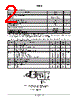
️· Oscillation Frequency: Adjustable via an external capacitor (Figure 16 shows frequency vs. capacitor value).
️· Source Resistance: The figure (Figure 15) illustrates its output source resistance versus temperature.
️· Load Regulation: Figure 22 indicates its output voltage behavior under varying load currents.
️· Temperature Dependence: Its characteristics (frequency, resistance) are impacted by temperature, as shown in Figures 17 and 15.
4. Circuit Configuration and Operation
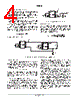
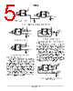
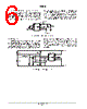
️· Charge Pumping: The core principle is charge pumping, which involves storing and transferring small amounts of charge to create a higher DC voltage.
️· External Components: External capacitors are crucial for setting the oscillation frequency and impacting voltage levels.
5. Package Information
️· Package Type: 8-Pin SOIC (Small Outline Integrated Circuit)
️· Dimensions: Detailed package dimensions are provided in the final section. These are key for PCB layout and physical integration.
6. Key Figures & Their Significance
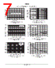
️· Figure 14 (Output Source Resistance vs. Supply Voltage): Shows how the regulator's ability to supply current changes with the input voltage.
️· Figure 15 (Output Source Resistance vs. Temperature): Demonstrates the temperature impact on its power delivery capability.
️· Figure 16 (Frequency vs. Oscillator Capacitance): Vital for setting the operating frequency by selecting appropriate external capacitors.
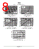
️· Figure 17 (Unloaded Oscillator Frequency vs. Temperature): Illustrates the frequency drift with temperature variations.
️· Figure 22 (Output Voltage vs. Load Current): Shows the regulator’s voltage stability under load.
In essence, the MC7660 is a versatile charge pump IC used to generate higher voltages from lower ones, offering flexibility in design and application.
1. Overview - What is the MC7660?
The MC7660 is a monolithic charge pump voltage regulator. In simpler terms, it's an integrated circuit (IC) that generates a higher voltage from a lower input voltage using a technique called charge pumping. This is useful for applications where a higher voltage is needed than what's readily available.
2. Key Features and Applications
️· Charge Pump Architecture: It utilizes a charge pump design, meaning it doesn't rely on a transformer to increase voltage.
️· Adjustable Output Voltage: It's designed to generate a higher voltage, which can be adjusted.
️· Applications: The document highlights it's suitable for a variety of applications, including:
- Non-volatile memory (EEPROM, Flash) programming
- LCD bias
- Set-top box power
- White LED Drivers
- Positive voltage generation
️· Versatility: It seems to be adaptable to different operating conditions and requirements.
3. Technical Specifications & Characteristics (based on figures & text)
️· Input Voltage Range: The document implies a range, but a precise minimum isn't specified.
️· Output Voltage: Adjustable (a key feature)
️· Oscillation Frequency: Adjustable via an external capacitor (Figure 16 shows frequency vs. capacitor value).
️· Source Resistance: The figure (Figure 15) illustrates its output source resistance versus temperature.
️· Load Regulation: Figure 22 indicates its output voltage behavior under varying load currents.
️· Temperature Dependence: Its characteristics (frequency, resistance) are impacted by temperature, as shown in Figures 17 and 15.
4. Circuit Configuration and Operation
️· Charge Pumping: The core principle is charge pumping, which involves storing and transferring small amounts of charge to create a higher DC voltage.
️· External Components: External capacitors are crucial for setting the oscillation frequency and impacting voltage levels.
5. Package Information
️· Package Type: 8-Pin SOIC (Small Outline Integrated Circuit)
️· Dimensions: Detailed package dimensions are provided in the final section. These are key for PCB layout and physical integration.
6. Key Figures & Their Significance
️· Figure 14 (Output Source Resistance vs. Supply Voltage): Shows how the regulator's ability to supply current changes with the input voltage.
️· Figure 15 (Output Source Resistance vs. Temperature): Demonstrates the temperature impact on its power delivery capability.
️· Figure 16 (Frequency vs. Oscillator Capacitance): Vital for setting the operating frequency by selecting appropriate external capacitors.
️· Figure 17 (Unloaded Oscillator Frequency vs. Temperature): Illustrates the frequency drift with temperature variations.
️· Figure 22 (Output Voltage vs. Load Current): Shows the regulator’s voltage stability under load.
In essence, the MC7660 is a versatile charge pump IC used to generate higher voltages from lower ones, offering flexibility in design and application.
| Part No. | MC7660 |
| Manufacturer | ONSEMI |
| Size | 191 Kbytes |
| Pages | 12 pages |
| Description | Charge Pump DC-to-DC Voltage Converter |
| ¿ALLDATASHEET es útil para Ud.? [ DONATE ] |
Todo acerca de Alldatasheet | Publicidad | Contáctenos | Política de Privacidad | Enlace a la hoja de datos | Intercambio de Enlaces | Lista de Fabricantes All Rights Reserved©Alldatasheet.com |
| Russian : Alldatasheetru.com | Korean : Alldatasheet.co.kr | Spanish : Alldatasheet.es | French : Alldatasheet.fr | Italian : Alldatasheetit.com Portuguese : Alldatasheetpt.com | Polish : Alldatasheet.pl | Vietnamese : Alldatasheet.vn Indian : Alldatasheet.in | Mexican : Alldatasheet.com.mx | British : Alldatasheet.co.uk | New Zealand : Alldatasheet.co.nz |
|
Family Site : ic2ic.com |
icmetro.com |
 Spanish ▼
  English
 Chinese
 German
 Japanese
 Russian
 Korean
 French
 Italian
 Portuguese
 Polish
 Vietnamese
 Indian
 Mexican
 British
 New Zealand