 |
Motor de Búsqueda de Datasheet de Componentes Electrónicos |
|
|
Motor de Búsqueda de Datasheet de Componentes Electrónicos |
|
The question interval is too short.
Please try again in a few seconds.

Hello, Please ask a question about CS1180 Datasheet
# Example questions:
➢ What is the minimum sclk high or low pulse width required for proper communication with the cs1180?
➢ What are the typical supply voltage ranges for the cs1180 when operating with a 3v supply, and what are the corresponding analog input ranges?
➢ What is the minimum time that the cs (chip select) signal must be held low after the last sclk clock edge to ensure proper data transfer, according to the provided timing table?
| Part No. | CS1180 |
| Manufacturer | CHIPSEA |
| Size | 757 Kbytes |
| Pages | 30 pages |
| Description | 20-bit Sigma-Delta ADC |



1. Overview
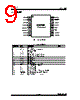
The CS1180 is an analog-to-digital converter (ADC) likely intended for precision measurement and data acquisition applications. It appears to be a versatile device with communication protocols and configurable parameters.
2. Power Supply & Voltage Ranges:
️· AVDD: Supports two operating voltages: 3V and 3.3V. This influences the range of analog input signals.
3. Electrical Characteristics:
️· Analog Input Ranges:
- *Buffer Enabled*: The input signal range is AGND - 0.1V to AVDD + 0.1V (with 3V or 6.6V supply)
- *Buffer Disabled*: The input signal range is AGND + 0.4V to AVDD - 1.5V (with 3V or 6.6V supply).
️· Resolution: 20-bit resolution.
️· Input Leakage Current: 5 pA (when the converter is in a defined state).
️· Dynamic Range (related to conversion): t6 allows a change of 5000 Tosc, where Tosc is the clock period.
️· Data Output: SDO (Serial Data Output) with a delay of 50ns relative to the SCLK (Serial Clock).
4. Communication & Timing
️· Serial Communication: Utilizes serial communication via SCLK and SDI (Serial Data In).
️· Communication Timing Parameters (Key Points):
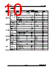
- `tspw` (SCLK Pulse Width): Minimum 200ns.
- `tcs1`: Setup time between CS falling edge and the first SCLK.
- `tds`: Data setup time (delay of SDI data relative to SCLK).
- `tdh`: Data hold time for SDI data.
- `tdio`: Data output delay (for operations like RDATA, RREG, WREG).
- `tdso`: Delay between SCLK and SDO data.
- `t6`: Maximum change in analog input signal allowed before the next conversion.
- `t8`: Delay between DRDY going low and the first SCLK.
️· Instruction Timing: Different instructions (GCALSELF, SELFOCAL, RESET) have varying delays between instruction completion and the start of the next instruction. This is controlled by `tsdelay`.
5. Key Features & Commands:
️· Programmable Gain Amplifier (PGA): Supports gain settings of 1 to 128.
️· Calibration Commands: Includes commands for self-calibration (`GCALSELF`, `SELFOCAL`, `GCALSYS`) to improve accuracy.
️· Sleep Mode: Suggests a low-power sleep mode is available.
️· DRDY Signal: The DRDY signal indicates when new data is ready.
️· Reset Functionality: Can be reset through SCLK or RST pin.
6. Considerations:
️· Power Supply Sensitivity: The performance characteristics (linearity, accuracy) are dependent on the supply voltage (3V or 3.3V). Careful power supply regulation is important.
️· Timing Constraints: Meeting the timing specifications (setup and hold times, data delays) is crucial for reliable serial communication.
️· Analog Signal Conditioning: The input signal must be properly conditioned (filtered, amplified, biased) to match the input range and dynamic requirements.
1. Overview
The CS1180 is an analog-to-digital converter (ADC) likely intended for precision measurement and data acquisition applications. It appears to be a versatile device with communication protocols and configurable parameters.
2. Power Supply & Voltage Ranges:
️· AVDD: Supports two operating voltages: 3V and 3.3V. This influences the range of analog input signals.
3. Electrical Characteristics:
️· Analog Input Ranges:
- *Buffer Enabled*: The input signal range is AGND - 0.1V to AVDD + 0.1V (with 3V or 6.6V supply)
- *Buffer Disabled*: The input signal range is AGND + 0.4V to AVDD - 1.5V (with 3V or 6.6V supply).
️· Resolution: 20-bit resolution.
️· Input Leakage Current: 5 pA (when the converter is in a defined state).
️· Dynamic Range (related to conversion): t6 allows a change of 5000 Tosc, where Tosc is the clock period.
️· Data Output: SDO (Serial Data Output) with a delay of 50ns relative to the SCLK (Serial Clock).
4. Communication & Timing
️· Serial Communication: Utilizes serial communication via SCLK and SDI (Serial Data In).
️· Communication Timing Parameters (Key Points):
- `tspw` (SCLK Pulse Width): Minimum 200ns.
- `tcs1`: Setup time between CS falling edge and the first SCLK.
- `tds`: Data setup time (delay of SDI data relative to SCLK).
- `tdh`: Data hold time for SDI data.
- `tdio`: Data output delay (for operations like RDATA, RREG, WREG).
- `tdso`: Delay between SCLK and SDO data.
- `t6`: Maximum change in analog input signal allowed before the next conversion.
- `t8`: Delay between DRDY going low and the first SCLK.
️· Instruction Timing: Different instructions (GCALSELF, SELFOCAL, RESET) have varying delays between instruction completion and the start of the next instruction. This is controlled by `tsdelay`.
5. Key Features & Commands:
️· Programmable Gain Amplifier (PGA): Supports gain settings of 1 to 128.
️· Calibration Commands: Includes commands for self-calibration (`GCALSELF`, `SELFOCAL`, `GCALSYS`) to improve accuracy.
️· Sleep Mode: Suggests a low-power sleep mode is available.
️· DRDY Signal: The DRDY signal indicates when new data is ready.
️· Reset Functionality: Can be reset through SCLK or RST pin.
6. Considerations:
️· Power Supply Sensitivity: The performance characteristics (linearity, accuracy) are dependent on the supply voltage (3V or 3.3V). Careful power supply regulation is important.
️· Timing Constraints: Meeting the timing specifications (setup and hold times, data delays) is crucial for reliable serial communication.
️· Analog Signal Conditioning: The input signal must be properly conditioned (filtered, amplified, biased) to match the input range and dynamic requirements.
| Part No. | CS1180 |
| Manufacturer | CHIPSEA |
| Size | 757 Kbytes |
| Pages | 30 pages |
| Description | 20-bit Sigma-Delta ADC |
| ¿ALLDATASHEET es útil para Ud.? [ DONATE ] |
Todo acerca de Alldatasheet | Publicidad | Contáctenos | Política de Privacidad | Enlace a la hoja de datos | Intercambio de Enlaces | Lista de Fabricantes All Rights Reserved©Alldatasheet.com |
| Russian : Alldatasheetru.com | Korean : Alldatasheet.co.kr | Spanish : Alldatasheet.es | French : Alldatasheet.fr | Italian : Alldatasheetit.com Portuguese : Alldatasheetpt.com | Polish : Alldatasheet.pl | Vietnamese : Alldatasheet.vn Indian : Alldatasheet.in | Mexican : Alldatasheet.com.mx | British : Alldatasheet.co.uk | New Zealand : Alldatasheet.co.nz |
|
Family Site : ic2ic.com |
icmetro.com |
 Spanish ▼
  English
 Chinese
 German
 Japanese
 Russian
 Korean
 French
 Italian
 Portuguese
 Polish
 Vietnamese
 Indian
 Mexican
 British
 New Zealand