|
Motor de Búsqueda de Datasheet de Componentes Electrónicos |
|
|
Motor de Búsqueda de Datasheet de Componentes Electrónicos |
|
HIP2103-4DEMO2Z Datasheet(PDF) 25 Page - Renesas Technology Corp |
|
|
|||||||||||||||||||||||||||||
HIP2103-4DEMO2Z Datasheet(HTML) 25 Page - Renesas Technology Corp |
|
|
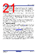
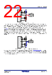
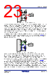
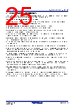
25 / 31 page  HIP2103, HIP2104 7. General PCB Layout Guidelines FN8276 Rev.2.0 Page 25 of 30 Feb 25, 2021 7. General PCB Layout Guidelines The AC performance of the HIP2103 and HIP2104 depends significantly on the design of the PCB. The following layout design guidelines are recommended to achieve optimum performance: • Place the driver as close as possible to the driven power FET. • Understand where the switching power currents flow. The high amplitude di/dt currents of the driven power FET induce significant voltage transients on the associated traces. • Keep power loops as short as possible by paralleling the source and return traces. • Use planes where practical; they are usually more effective than parallel traces. • Avoid paralleling high amplitude di/dt traces with low level signal lines. High di/dt induces currents and consequently, noise voltages in the low level signal lines. • When practical, minimize impedances in low-level signal circuits. Magnetically induced noise on a 10kΩ resistor, is 10x larger than the noise on a 1kΩ resistor. • Be aware of magnetic fields emanating from motors and inductors. Gaps in the magnetic cores of these structures are especially bad for emitting flux. • If you must have traces close to magnetic devices, align the traces so that they are parallel to the flux lines to minimize coupling. • The use of low inductance components such as chip resistors and chip capacitors is highly recommended. • Use decoupling capacitors to reduce the influence of parasitic inductance in the VBAT, VDD, and GND leads. To be effective, these capacitors must also have the shortest possible conduction paths. If vias are used, connect several paralleled vias to reduce the inductance of the vias. • It may be necessary to add resistance to dampen resonating parasitic circuits, especially on LO and LO. If an external gate resistor is unacceptable, the layout must be improved to minimize lead inductance. • Keep high dv/dt nodes away from low level circuits. Use guard banding to shunt away dv/dt injected currents from sensitive circuits. • Avoid having a signal ground plane under a high amplitude dv/dt circuit. The parasitic capacitance of a ground plane, Cp, relative to the high amplitude dv/dt circuit results in injected (Cp x dv/dt) currents into the signal ground paths where C is the parasitic capacitance of the ground plane. • Do power dissipation and voltage drop calculations of the power traces. Many PCB/CAD programs have built in tools for calculation of trace resistance. The internet is also a good source for resistance calculators for PCB trace resistance. • Large power components (such as power FETs, electrolytic capacitors, and power resistors) have internal parasitic inductance that cannot be eliminated. This must be accounted for in the PCB layout and circuit design. • If you simulate your circuits, consider including parasitic components, especially parasitic inductance. |
|
Enlace URL |
| ¿ALLDATASHEET es útil para Ud.? [ DONATE ] |
Todo acerca de Alldatasheet | Publicidad | Contáctenos | Política de Privacidad | Enlace a la hoja de datos | Intercambio de Enlaces | Lista de Fabricantes All Rights Reserved©Alldatasheet.com |
| Russian : Alldatasheetru.com | Korean : Alldatasheet.co.kr | Spanish : Alldatasheet.es | French : Alldatasheet.fr | Italian : Alldatasheetit.com Portuguese : Alldatasheetpt.com | Polish : Alldatasheet.pl | Vietnamese : Alldatasheet.vn Indian : Alldatasheet.in | Mexican : Alldatasheet.com.mx | British : Alldatasheet.co.uk | New Zealand : Alldatasheet.co.nz |
|
Family Site : ic2ic.com |
icmetro.com |
 Spanish ▼
 English
 Chinese
 German
 Japanese
 Russian
 Korean
 Spanish
 French
 Italian
 Portuguese
 Polish
 Vietnamese
 Indian
 Mexican
 British
 New Zealand