|
Motor de Búsqueda de Datasheet de Componentes Electrónicos |
|
|
Motor de Búsqueda de Datasheet de Componentes Electrónicos |
|
LTC2420CS8 Datasheet(PDF) 29 Page - Linear Technology |
|
|
|||||||||||||||||||||||||||||
LTC2420CS8 Datasheet(HTML) 29 Page - Linear Technology |
|
|
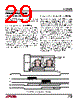
29 / 36 page  29 LTC2420 SYNCHRONIZATION OF MULTIPLE LTC2420s Since the LTC2420’s absolute accuracy (total unadjusted error) is 10ppm, applications utilizing multiple matched ADCs are possible. Simultaneous Sampling with Two LTC2420s One such application is synchronizing multiple LTC2420s, see Figure 35. The start of conversion is synchronized to the rising edge of CS. In order to synchronize multiple LTC2420s, CS is a common input to all the ADCs. To prevent the converters from autostarting a new con- version at the end of data output read, 23 or fewer SCK clock signals are applied to the LTC2420 instead of 24 (the 24th falling edge would start a conversion). The exact timing and frequency for the SCK signal is not critical since it is only shifting out the data. In this case, two LTC2420’s simultaneously start and end their conversion cycles under the external control of CS. TYPICAL APPLICATIO S Increasing the Output Rate Using Multiple LTC2420s A second application uses multiple LTC2420s to increase the effective output rate by 4 ×, see Figure 36. In this case, four LTC2420s are interleaved under the control of sepa- rate CS signals. This increases the effective output rate from 7.5Hz to 30Hz (up to a maximum of 400Hz). Addi- tionally, the one-shot output spectrum is unfolded allow- ing further digital signal processing of the conversion results. SCK and SDO may be common to all four LTC2420s. The four CS rising edges equally divide one LTC2420 conversion cycle (7.5Hz for 60Hz notch frequency). In order to synchronize the start of conversion to CS, 23 or less SCK clock pulses must be applied to each ADC. Both the synchronous and 4 × output rate applications use the external serial clock and single cycle operation with reduced data output length (see Serial Interface Timing Modes section and Figure 7). An external oscillator clock is applied commonly to the FO pin of each LTC2420 in order to synchronize the sampling times. Both circuits may be extended to include more LTC2420s. 23 OR LESS CLOCK CYCLES CS SCK1 SCK2 2420 F35 SDO1 SDO2 23 OR LESS CLOCK CYCLES LTC2420 #1 VCC VREF VIN GND FO SCK SDO CS SCK2 SCK1 CS SDO1 SDO2 LTC2420 #2 VCC VREF VIN GND FO SCK SDO CS µCONTROLLER EXTERNAL OSCILLATOR (153,600HZ) VREF (0.1V TO VCC) Figure 35. Synchronous Conversion—Extendable |
|
Enlace URL |
| ¿ALLDATASHEET es útil para Ud.? [ DONATE ] |
Todo acerca de Alldatasheet | Publicidad | Contáctenos | Política de Privacidad | Enlace a la hoja de datos | Intercambio de Enlaces | Lista de Fabricantes All Rights Reserved©Alldatasheet.com |
| Russian : Alldatasheetru.com | Korean : Alldatasheet.co.kr | Spanish : Alldatasheet.es | French : Alldatasheet.fr | Italian : Alldatasheetit.com Portuguese : Alldatasheetpt.com | Polish : Alldatasheet.pl | Vietnamese : Alldatasheet.vn Indian : Alldatasheet.in | Mexican : Alldatasheet.com.mx | British : Alldatasheet.co.uk | New Zealand : Alldatasheet.co.nz |
|
Family Site : ic2ic.com |
icmetro.com |
 Spanish ▼
 English
 Chinese
 German
 Japanese
 Russian
 Korean
 Spanish
 French
 Italian
 Portuguese
 Polish
 Vietnamese
 Indian
 Mexican
 British
 New Zealand