|
Motor de Búsqueda de Datasheet de Componentes Electrónicos |
|
|
Motor de Búsqueda de Datasheet de Componentes Electrónicos |
|
LTC2420CS8 Datasheet(PDF) 23 Page - Linear Technology |
|
|
|||||||||||||||||||||||||||||
LTC2420CS8 Datasheet(HTML) 23 Page - Linear Technology |
|
|
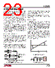
23 / 36 page  23 LTC2420 propagation delay from the driver to LTC2420. For refer- ence, on a regular FR-4 board, signal propagation veloc- ity is approximately 183ps/inch for internal traces and 170ps/inch for surface traces. Thus, a driver generating a control signal with a minimum transition time of 1ns must be connected to the converter pin through a trace shorter than 2.5 inches. This problem becomes particu- larly difficult when shared control lines are used and multiple reflections may occur. The solution is to care- fully terminate all transmission lines close to their char- acteristic impedance. Parallel termination near the LTC2420 pin will eliminate this problem but will increase the driver power dissipation. A series resistor between 27 Ω and 56Ω placed near the driver or near the LTC2420 pin will also eliminate this problem without additional power dissipation. The actual resistor value depends upon the trace impedance and connection topology. Driving the Input and Reference The analog input and reference of the typical delta-sigma analog-to-digital converter are applied to a switched ca- pacitor network. This network consists of capacitors switch- ing between the analog input (VIN), ground (Pin 4) and the reference (VREF). The result is small current spikes seen at both VIN and VREF. A simplified input equivalent circuit is shown in Figure 16. The key to understanding the effects of this dynamic input current is based on a simple first order RC time constant model. Using the internal oscillator, the LTC2420’s inter- nal switched capacitor network is clocked at 153,600Hz corresponding to a 6.5 µs sampling period. Fourteen time constants are required each time a capacitor is switched in order to achieve 1ppm settling accuracy. Therefore, the equivalent time constant at VIN and VREF should be less than 6.5 µs/14 = 460ns in order to achieve 1ppm accuracy. Input Current (VIN) If complete settling occurs on the input, conversion re- sults will be uneffected by the dynamic input current. If the settling is incomplete, it does not degrade the linearity performance of the device. It simply results in an offset/ full-scale shift, see Figure 17. To simplify the analysis of input dynamic current, two separate cases are assumed: large capacitance at VIN (CIN > 0.01µF) and small capaci- tance at VIN (CIN < 0.01µF). If the total capacitance at VIN (see Figure 18) is small (< 0.01 µF), relatively large external source resistances (up to 80k for 20pF parasitic capacitance) can be tolerated without any offset/full-scale error. Figures 19 and 20 show a family of offset and full-scale error curves for various small valued input capacitors (CIN < 0.01µF) as a function of input source resistance. APPLICATIO S I FOR ATIO VREF VIN VCC RSW 5k AVERAGE INPUT CURRENT: IIN = 0.25(VIN – 0.5 • VREF)fCEQ IREF(LEAK) IREF(LEAK) VCC RSW 5k CEQ 1pF (TYP) RSW 5k IIN(LEAK) IIN 2420 F16 IIN(LEAK) SWITCHING FREQUENCY f = 153.6kHz FOR INTERNAL OSCILLATOR (fO = LOGIC LOW OR HIGH) f = fEOSC FOR EXTERNAL OSCILLATORS GND Figure 16. LTC2420 Equivalent Analog Input Circuit 0 TUE VREF/2 VIN 2420 F17 VREF CIN 2420 F18 INTPUT SIGNAL SOURCE RSOURCE VIN LTC2420 CPAR ≅20pF Figure 17. Offset/Full-Scale Shift Figure 18. An RC Network at VIN |
|
Enlace URL |
| ¿ALLDATASHEET es útil para Ud.? [ DONATE ] |
Todo acerca de Alldatasheet | Publicidad | Contáctenos | Política de Privacidad | Enlace a la hoja de datos | Intercambio de Enlaces | Lista de Fabricantes All Rights Reserved©Alldatasheet.com |
| Russian : Alldatasheetru.com | Korean : Alldatasheet.co.kr | Spanish : Alldatasheet.es | French : Alldatasheet.fr | Italian : Alldatasheetit.com Portuguese : Alldatasheetpt.com | Polish : Alldatasheet.pl | Vietnamese : Alldatasheet.vn Indian : Alldatasheet.in | Mexican : Alldatasheet.com.mx | British : Alldatasheet.co.uk | New Zealand : Alldatasheet.co.nz |
|
Family Site : ic2ic.com |
icmetro.com |
 Spanish ▼
 English
 Chinese
 German
 Japanese
 Russian
 Korean
 Spanish
 French
 Italian
 Portuguese
 Polish
 Vietnamese
 Indian
 Mexican
 British
 New Zealand