|
Motor de Búsqueda de Datasheet de Componentes Electrónicos |
|
|
Motor de Búsqueda de Datasheet de Componentes Electrónicos |
|
M30620FCAFP Datasheet(PDF) 22 Page - Mitsubishi Electric Semiconductor |
|
|
|||||||||||||||||||||||||||||
M30620FCAFP Datasheet(HTML) 22 Page - Mitsubishi Electric Semiconductor |
|
|
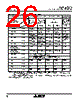
22 / 274 page  Mitsubishi microcomputers M16C / 62A Group SINGLE-CHIP 16-BIT CMOS MICROCOMPUTER Processor Mode 22 Figure 1.7.1. Processor mode register 0 and 1 Processor mode register 0 (Note 1) Symbol Address When reset PM0 000416 0016 (Note 2) Bit name Function Bit symbol W R b7 b6 b5 b4 b3 b2 b1 b0 0 0: Single-chip mode 0 1: Memory expansion mode 1 0: Inhibited 1 1: Microprocessor mode b1 b0 PM03 PM01 PM00 Processor mode bit PM02 R/W mode select bit 0 : RD,BHE,WR 1 : RD,WRH,WRL Software reset bit The device is reset when this bit is set to “1”. The value of this bit is “0” when read. PM04 0 0 : Multiplexed bus is not used 0 1 : Allocated to CS2 space 1 0 : Allocated to CS1 space 1 1 : Allocated to entire space (Note4) b5 b4 Multiplexed bus space select bit PM05 PM06 PM07 Port P40 to P43 function select bit (Note 3) 0 : Address output 1 : Port function (Address is not output) BCLK output disable bit 0 : BCLK is output 1 : BCLK is not output (Pin is left floating) Note 1: Set bit 1 of the protect register (address 000A16) to “1” when writing new values to this register. Note 2: If the VCC voltage is applied to the CNVSS, the value of this register when reset is 0316. (PM00 and PM01 both are set to “1”.) Note 3: Valid in microprocessor and memory expansion modes. Note 4: If the entire space is of multiplexed bus in memory expansion mode, choose an 8- bit width.The processor operates using the separate bus after reset is revoked, so the entire space multiplexed bus cannot be chosen in microprocessor mode. The higher-order address becomes a port if the entire space multiplexed bus is chosen, so only 256 bytes can be used in each chip select. Processor mode register 1 (Note 1) Symbol Address When reset PM1 000516 00000XX02 Bit name Function Bit symbol W R b7 b6 b5 b4 b3 b2 b1 b0 Nothing is assigned. In an attempt to write to these bits, write “0”. The value, if read, turns out to be indeterminate. Reserved bit Must always be set to “0” 0 Note 1: Set bit 1 of the protect register (address 000A16) to “1” when writing new values to this register. Note 2: Be sure to set this bit to 0 except products whose RAM size and ROM size exceed 15K bytes and 192K bytes respectively. In using M30624MAG/FGA, a product having a RAM of more than 15K bytes and a ROM of more than 192K bytes, set this bit to “1” at the beginning of user program. Specify D000016 or a subsequent address, which becomes an internal ROM area if PM13 is set to “0” at the time reset is revoked, for the reset vector table of user program. PM17 Wait bit 0 : No wait state 1 : Wait state inserted Reserved bit Must always be set to “0” 0 Internal reserved area expansion bit (Note 2) PM13 0: The same internal reserved area as that of M16C/60 and M16C/61 group 1: Expands the internal RAM area and internal ROM area to 23 K bytes and to 256K bytes respectively. (Note 2) 00 Reserved bit Must always be set to “0” Reserved bit Must always be set to “0” |
|
Enlace URL |
| ¿ALLDATASHEET es útil para Ud.? [ DONATE ] |
Todo acerca de Alldatasheet | Publicidad | Contáctenos | Política de Privacidad | Enlace a la hoja de datos | Intercambio de Enlaces | Lista de Fabricantes All Rights Reserved©Alldatasheet.com |
| Russian : Alldatasheetru.com | Korean : Alldatasheet.co.kr | Spanish : Alldatasheet.es | French : Alldatasheet.fr | Italian : Alldatasheetit.com Portuguese : Alldatasheetpt.com | Polish : Alldatasheet.pl | Vietnamese : Alldatasheet.vn Indian : Alldatasheet.in | Mexican : Alldatasheet.com.mx | British : Alldatasheet.co.uk | New Zealand : Alldatasheet.co.nz |
|
Family Site : ic2ic.com |
icmetro.com |
 Spanish ▼
 English
 Chinese
 German
 Japanese
 Russian
 Korean
 Spanish
 French
 Italian
 Portuguese
 Polish
 Vietnamese
 Indian
 Mexican
 British
 New Zealand