|
Motor de Búsqueda de Datasheet de Componentes Electrónicos |
|
|
Motor de Búsqueda de Datasheet de Componentes Electrónicos |
|
AS1123 Datasheet(PDF) 13 Page - ams AG |
|
|
|||||||||||||||||||||||||||||
AS1123 Datasheet(HTML) 13 Page - ams AG |
|
|
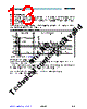
13 / 25 page  www.austriamicrosystems.com/LED-Driver-ICs Revision 1.00 12 - 24 AS1123 Datasheet - D e t a i l e d D e s c r i p t i o n Detailed Error Reports The detailed error report can be read out after global error mode has been run. At the falling edge of LD, the detailed error report of the selected test is latched into the shift register and can be clocked out with n*16 clock cycles (n is the number of AS1123s in a chain) via pin SDO. At the same time new data can be written into the shift register, which is loaded on the next rising edge of pin LD. This pattern is shown at the output drivers, at the falling edge of OEN. Detailed Temperature Warning Report The detailed temperature warning report can be read out immediately after global error mode has been run. SDI must be 1 for the first device. Bit0 of the 16bit data word represents the temperature flag of the chip. Figure 14. Detailed Temperature Warning Report Timing Diagram Detailed Temperature Warning Report Example: Consider a case where four AS1123s are cascaded in one chain. The detailed error report lists the temperatures for each device in the chain: IC1:[70°] IC2:[85°] IC3:[170°] IC4:[60°] In this case, IC3 is overheated and will generate a global error, and therefore 4*16 clock cycles are needed to write out the detailed temperature warning report, and optionally read in new data. The detailed temperature warning report would look like this: XXXXXXXXXXXXXXX1 XXXXXXXXXXXXXXX1 XXXXXXXXXXXXXXX0 XXXXXXXXXXXXXXX1 The 0 in the detailed temperature warning report indicates that IC3 is the device with the over-temperature condition. Note: In an actual report there are no spaces in the output. Global Flag Readout Detailed Error Report Readout tH(L) tP4 tP4 SDI OEN LD CLK SDO New Data Input TFLAG DBit15 Undefined Don’t Care Don’t Care Temperature Error Report Output DBit14 DBit13 DBit12 DBitn DBit2 DBit1 DBit0 TBit0 t(SU)ERROR tP1 For detailed timing information see Timing Diagrams on page 8. tGSW(ERROR) |
|
|
Enlace URL |
| ¿ALLDATASHEET es útil para Ud.? [ DONATE ] |
Todo acerca de Alldatasheet | Publicidad | Contáctenos | Política de Privacidad | Enlace a la hoja de datos | Intercambio de Enlaces | Lista de Fabricantes All Rights Reserved©Alldatasheet.com |
| Russian : Alldatasheetru.com | Korean : Alldatasheet.co.kr | Spanish : Alldatasheet.es | French : Alldatasheet.fr | Italian : Alldatasheetit.com Portuguese : Alldatasheetpt.com | Polish : Alldatasheet.pl | Vietnamese : Alldatasheet.vn Indian : Alldatasheet.in | Mexican : Alldatasheet.com.mx | British : Alldatasheet.co.uk | New Zealand : Alldatasheet.co.nz |
|
Family Site : ic2ic.com |
icmetro.com |
 Spanish ▼
 English
 Chinese
 German
 Japanese
 Russian
 Korean
 Spanish
 French
 Italian
 Portuguese
 Polish
 Vietnamese
 Indian
 Mexican
 British
 New Zealand