|
Motor de Búsqueda de Datasheet de Componentes Electrónicos |
|
|
Motor de Búsqueda de Datasheet de Componentes Electrónicos |
|
LTC3336ACBZ-2-R7 Datasheet(PDF) 16 Page - Analog Devices |
|
|
|||||||||||||||||||||||||||||
LTC3336ACBZ-2-R7 Datasheet(HTML) 16 Page - Analog Devices |
|
|
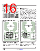
16 / 24 page  LTC3336 16 Rev. A For more information www.analog.com Figure 2. Recommended Component Placement on PCB for the LTC3336 in LQFN Package APPLICATIONS INFORMATION Figure 3. Recommended Component Placement on PCB for the LTC3336-1 or LTC3336-2 in WLCSP application: Microcontroller Supply with Dynamic Output Voltage Change in the Typical Applications section. Table 4. Dynamic Operation Output Voltages with Single Pin Tied High PIN TIED HIGH (DEFAULT) VDEFAULT (V) DYNAMIC OUTPUT VOLTAGES AVAILABLE WITH SINGLE PIN TIED HIGH (V) OUT0 1.2 1.2, 1.5, 2.4, 2.8, 3.3, 3.7, 4.1, 5.0 OUT1 1.8 1.5, 1.8, 2.0, 2.8, 3.6, 3.7, 4.2, 5.0 OUT2 2.5 2.0, 2.4, 2.5, 2.8, 3.2, 4.1, 4.2, 5.0 OUT3 3.0 3.0, 3.2, 3.3, 3.6, 3.7, 4.1, 4.2, 5.0 PCB Layout Considerations The LTC3336 switches large currents (relative to the IQ) at high frequencies. Special care should be given to the PCB layout to ensure stable, noise-free operation. Figure 2 and Figure 3 depict recommended PCB layout to be uti- lized for the LTC3336, in the QFN and WLCSP packages, respectively. A few key guidelines follow: All circulating high current paths should be kept as short as possible using wide traces. In particular, capacitor ground connec- tions should connect by vias down to the ground plane in the shortest route possible. The bypass capacitors CIN and COUT should be placed as close to the IC as possible. COUT CIN 10 9 8 7 1 2 3 4 12 11 5 6 L LPS4018 LTC3336 TOP LAYER BOTTOM COPPER LAYER (GROUND PLANE) CONNECTED TO GND VIN EN IPK1 IPK0 OUT0 OUT1 OUT2 OUT3 GND SEE TYPICAL APPLICATION ON FRONT PAGE VIAS TO GROUND PLANE COMPONENT SIZES: CIN = 0201 COUT = 1210 3336 F02 TOP LAYER SEE TYPICAL APPLICATION ON FRONT PAGE VIAS TO GROUND PLANE COMPONENT SIZES: CIN = 0201 CINTVCC = 0201 COUT = 1210 3336 F03 BOTTOM COPPER LAYER (GROUND PLANE) CONNECTED TO GND CINTVCC L LPS4018 LTC3336-2 A1 A2 A3 B1 B2 B3 C1 C2 C3 D1 D2 D3 COUT CIN |
|
|
Enlace URL |
| ¿ALLDATASHEET es útil para Ud.? [ DONATE ] |
Todo acerca de Alldatasheet | Publicidad | Contáctenos | Política de Privacidad | Enlace a la hoja de datos | Intercambio de Enlaces | Lista de Fabricantes All Rights Reserved©Alldatasheet.com |
| Russian : Alldatasheetru.com | Korean : Alldatasheet.co.kr | Spanish : Alldatasheet.es | French : Alldatasheet.fr | Italian : Alldatasheetit.com Portuguese : Alldatasheetpt.com | Polish : Alldatasheet.pl | Vietnamese : Alldatasheet.vn Indian : Alldatasheet.in | Mexican : Alldatasheet.com.mx | British : Alldatasheet.co.uk | New Zealand : Alldatasheet.co.nz |
|
Family Site : ic2ic.com |
icmetro.com |
 Spanish ▼
 English
 Chinese
 German
 Japanese
 Russian
 Korean
 Spanish
 French
 Italian
 Portuguese
 Polish
 Vietnamese
 Indian
 Mexican
 British
 New Zealand