|
Motor de Búsqueda de Datasheet de Componentes Electrónicos |
|
|
Motor de Búsqueda de Datasheet de Componentes Electrónicos |
|
LTC3336ACBZ-2-R7 Datasheet(PDF) 4 Page - Analog Devices |
|
|
|||||||||||||||||||||||||||||
LTC3336ACBZ-2-R7 Datasheet(HTML) 4 Page - Analog Devices |
|
|
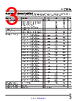
4 / 24 page  LTC3336 4 Rev. A For more information www.analog.com PARAMETER CONDITIONS MIN TYP MAX UNITS VOUT Pull-Down Resistor in Shutdown EN = 0V 10 kΩ VOUT Pull-Down Resistor in VOUT Overvoltage Condition 1 MΩ VOUT Overvoltage Detection Threshold as Percentage of Output Setting 5 % IPEAK (Inductor Peak Current) 10mA IPEAK Setting, ISW Rising 8.7 10 13 mA 30mA IPEAK Setting, ISW Rising 26 30 39 mA 100mA IPEAK Setting, ISW Rising 87 100 130 mA 300mA IPEAK Setting, ISW Rising 260 300 390 mA IVALLEY (Inductor Valley Current) 10mA IPEAK Setting, ISW Falling 9 mA 30mA IPEAK Setting, ISW Falling 27 mA 100mA IPEAK Setting, ISW Falling 90 mA 300mA IPEAK Setting, ISW Falling 270 mA Deliverable Output Current 10mA IPEAK Setting l 8.3 mA 30mA IPEAK Setting l 25 mA 100mA IPEAK Setting l 83 mA 300mA IPEAK Setting l 250 mA IZERO Inductor Current Going into Sleep, as a Percentage of IPEAK 17 % P-Channel MOSFET Switch On-Resistance 10mA IPEAK Setting 16 Ω 30mA IPEAK Setting 5.3 Ω 100mA IPEAK Setting 1.6 Ω 300mA IPEAK Setting 0.53 Ω N-Channel MOSFET Switch On-Resistance 10mA IPEAK Setting, 5V VOUT Setting 9.6 Ω 30mA IPEAK Setting, 5V VOUT Setting 3.2 Ω 100mA IPEAK Setting, 5V VOUT Setting 0.96 Ω 300mA IPEAK Setting, 5V VOUT Setting 0.32 Ω P-Channel MOSFET Switch Leakage 0 15 nA N-Channel MOSFET Switch Leakage 0 15 nA INTVCC Voltage VOUT Settings < 2.4V, 0 ≤ I(INTVCC) ≤ 10µA 1.9 2 2.2 V VOUT Settings ≥ 2.4V, 0 ≤ I(INTVCC) ≤ 10µA VOUT V VUVLO Undervoltage Lockout VIN Rising 1.95 2.2 V VIN Falling 1.5 1.75 V VIH Digital Input High Voltage Pins EN, IPK[1:0] INTVCC – 0.15V V Pins OUT[3:0] VOUT – 0.15V V VIL Digital Input Low Voltage Pins EN, IPK[1:0], OUT[3:0] 0.15 V ELECTRICAL CHARACTERISTICS The l denotes the specifications which apply over the specified operating junction temperature range, otherwise specifications are at TA = 25°C (Note 2). VIN = 7.2V unless otherwise noted. Note 1: Stresses beyond those listed under Absolute Maximum Ratings may cause permanent damage to the device. Exposure to any Absolute Maximum Rating condition for extended periods may affect device reliability and lifetime. Note 2: The LTC3336 is specified over the –40°C to 125°C operating junction temperature range. High junction temperatures degrade operating lifetimes. Note the maximum ambient temperature consistent with these specifications is determined by specific operating conditions in conjunction with board layout, the rated package thermal impedance and other environmental factors. Note 3: TJ is calculated from the ambient TA and power dissipation PD according to the following formula: TJ = TA + (PD • θJA). Note 4: Dynamic supply current is higher due to gate charge being delivered at the switching frequency. Note 5: The falling threshold is specified as a percentage of the average of the measured sleep and wake-up thresholds for each selected output voltage and the rising threshold is equal to the sleep threshold. |
|
|
Enlace URL |
| ¿ALLDATASHEET es útil para Ud.? [ DONATE ] |
Todo acerca de Alldatasheet | Publicidad | Contáctenos | Política de Privacidad | Enlace a la hoja de datos | Intercambio de Enlaces | Lista de Fabricantes All Rights Reserved©Alldatasheet.com |
| Russian : Alldatasheetru.com | Korean : Alldatasheet.co.kr | Spanish : Alldatasheet.es | French : Alldatasheet.fr | Italian : Alldatasheetit.com Portuguese : Alldatasheetpt.com | Polish : Alldatasheet.pl | Vietnamese : Alldatasheet.vn Indian : Alldatasheet.in | Mexican : Alldatasheet.com.mx | British : Alldatasheet.co.uk | New Zealand : Alldatasheet.co.nz |
|
Family Site : ic2ic.com |
icmetro.com |
 Spanish ▼
 English
 Chinese
 German
 Japanese
 Russian
 Korean
 Spanish
 French
 Italian
 Portuguese
 Polish
 Vietnamese
 Indian
 Mexican
 British
 New Zealand