|
Motor de Búsqueda de Datasheet de Componentes Electrónicos |
|
|
Motor de Búsqueda de Datasheet de Componentes Electrónicos |
|
ADUM7703 Datasheet(PDF) 10 Page - Analog Devices |
|
|
|||||||||||||||||||||||||||||
ADUM7703 Datasheet(HTML) 10 Page - Analog Devices |
|
|
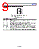
10 / 22 page  ADuM7703 Data Sheet Rev. A | Page 10 of 22 VDD1 1 VIN+ 2 VIN– 3 GND1 4 MDAT 8 GND2 7 VDD2 6 MCLKIN 5 ADuM7703 TOP VIEW (Not to Scale) NOTES 1. CONNECT GND1 BEFORE VDD1. Figure 6. 8-Lead SOIC_IC Pin Configuration Table 12. 8-Lead SOIC_IC Pin Function Descriptions Pin No. Mnemonic Description 1 VDD1 Supply Voltage, 4.5 V to 20 V. This pin is the supply voltage for the isolated side of the ADuM7703 and is relative to GND1. For device operation, connect the VDD1 supply voltage to the VDD1 pin. Decouple the supply pin to GND1 with a 10 μF capacitor in parallel with a 100 nF capacitor as close to the pin as possible. 2 VIN+ Positive Analog Input. 3 VIN− Negative Analog Input. 4 GND1 Ground 1. This pin is the ground reference point for all circuitry on the isolated side. 5 GND2 Ground 2. This pin is the ground reference point for all circuitry on the nonisolated side. 6 MDAT Serial Data Output. The single-bit modulator output is supplied to this pin as a serial data stream. The bits are clocked out on the rising edge of the MCLKIN input and are valid on the following MCLKIN rising edge. 7 MCLKIN Master Clock Logic Input, 5 MHz to 21 MHz frequency range. The bit stream from the modulator is propagated on the rising edge of the MCLKIN. 8 VDD2 Supply Voltage, 3 V or 5.5 V. This pin is the supply voltage for the nonisolated side and is relative to GND2. Decouple this supply to GND2 with a 10 μF capacitor in parallel with a 100 nF capacitor as close to the pin as possible. |
|
|
Enlace URL |
| ¿ALLDATASHEET es útil para Ud.? [ DONATE ] |
Todo acerca de Alldatasheet | Publicidad | Contáctenos | Política de Privacidad | Enlace a la hoja de datos | Intercambio de Enlaces | Lista de Fabricantes All Rights Reserved©Alldatasheet.com |
| Russian : Alldatasheetru.com | Korean : Alldatasheet.co.kr | Spanish : Alldatasheet.es | French : Alldatasheet.fr | Italian : Alldatasheetit.com Portuguese : Alldatasheetpt.com | Polish : Alldatasheet.pl | Vietnamese : Alldatasheet.vn Indian : Alldatasheet.in | Mexican : Alldatasheet.com.mx | British : Alldatasheet.co.uk | New Zealand : Alldatasheet.co.nz |
|
Family Site : ic2ic.com |
icmetro.com |
 Spanish ▼
 English
 Chinese
 German
 Japanese
 Russian
 Korean
 Spanish
 French
 Italian
 Portuguese
 Polish
 Vietnamese
 Indian
 Mexican
 British
 New Zealand