|
Motor de Búsqueda de Datasheet de Componentes Electrónicos |
|
|
Motor de Búsqueda de Datasheet de Componentes Electrónicos |
|
M30620FCAFP Datasheet(PDF) 142 Page - Mitsubishi Electric Semiconductor |
|
|
|||||||||||||||||||||||||||||
M30620FCAFP Datasheet(HTML) 142 Page - Mitsubishi Electric Semiconductor |
|
|
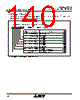
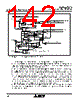
142 / 274 page  Mitsubishi microcomputers M16C / 62A Group SINGLE-CHIP 16-BIT CMOS MICROCOMPUTER UART2 Special Mode Register 2 142 P70/TxD2/SDA P71/RxD2/SCL CLK control P72/CLK2 Falling edge detection UART2 reception/ACK interrupt request, DMA1 request To DMA0, DMA1 To DMA0 2 P70 through P72 conforming to the simplified I C bus I/O Timer UART2 Timer UART2 IICM=1 (SDDS=0) or DL=000 (SDDS=1) IICM=0 or IICM2=1 IICM=1 and IICM2=0 SDHI Noize Filter Timer UART2 UART2 I/O D T Q D T Q D T Q NACK ACK UART2 UART2 IICM=1 IICM=0 IICM=0 IICM=1 IICM=1 IICM=0 S R Q IICM=1 IICM=0 I/O R Q ALS IICM=0 or DL ≠000 (SDDS=1) SDDS=0 or DL=000 SDDS=1 and DL ≠000 SWC2 Falling edge of 9 bit SWC IICM=1 and IICM2=0 IICM=0 or IICM2=1 Selector Selector Selector Noize Filter Noize Filter * With IICM set to 1, the port terminal is to be readable even if 1 is assigned to P7 1 of the direction register. Port reading External clock Internal clock 9th pulse Bus collision detection Bus collision/start, stop condition detection interrupt request UART2 transmission/ NACK interrupt request Start condition detection Stop condition detection L-synchronous output enabling bit (Port P71 output data latch) Data bus Reception register Bus busy Transmission register Arbitration Analog delay Digital delay (Divider) Functions available in I2C mode are shown in Figure 1.16.30 — a functional block diagram. Bit 3 of the UART2 special mode register 2 (address 037616) is used as the SDA output stop bit. Setting this bit to “1” causes an arbitration loss to occur, and the SDA pin turns to high-impedance state at the instant when the arbitration lost detecting flag is set to “1”. Bit 1 of the UART2 special mode register 2 (address 037616) is used as the clock synchronization bit. With this bit set to “1” at the time when the internal SCL is set to “H”, the internal SCL turns to “L” if the falling edge is found in the SCL pin; and the baud rate generator reloads the set value, and start counting within the “L” interval. When the internal SCL changes from “L” to “H” with the SCL pin set to “L”, stops counting the baud rate generator, and starts counting it again when the SCL pin turns to “H”. Due to this function, the UART2 transmission-reception clock becomes the logical product of the signal flowing through the internal SCL and that flowing through the SCL pin. This function operates over the period from the moment earlier by a half cycle than falling edge of the UART2 first clock to the rising edge of the ninth bit. To use this function, choose the internal clock for the transfer clock. Bit 2 of the UART2 special mode register 2 (037616) is used as the SCL wait output bit. Setting this bit to “1” causes the SCL pin to be fixed to “L” at the falling edge of the ninth bit of the clock. Setting this bit to “0” frees the output fixed to “L”. Figure 1.16.30. Functional block diagram for I2C mode |
|
Enlace URL |
| ¿ALLDATASHEET es útil para Ud.? [ DONATE ] |
Todo acerca de Alldatasheet | Publicidad | Contáctenos | Política de Privacidad | Enlace a la hoja de datos | Intercambio de Enlaces | Lista de Fabricantes All Rights Reserved©Alldatasheet.com |
| Russian : Alldatasheetru.com | Korean : Alldatasheet.co.kr | Spanish : Alldatasheet.es | French : Alldatasheet.fr | Italian : Alldatasheetit.com Portuguese : Alldatasheetpt.com | Polish : Alldatasheet.pl | Vietnamese : Alldatasheet.vn Indian : Alldatasheet.in | Mexican : Alldatasheet.com.mx | British : Alldatasheet.co.uk | New Zealand : Alldatasheet.co.nz |
|
Family Site : ic2ic.com |
icmetro.com |
 Spanish ▼
 English
 Chinese
 German
 Japanese
 Russian
 Korean
 Spanish
 French
 Italian
 Portuguese
 Polish
 Vietnamese
 Indian
 Mexican
 British
 New Zealand