|
Motor de Búsqueda de Datasheet de Componentes Electrónicos |
|
|
Motor de Búsqueda de Datasheet de Componentes Electrónicos |
|
LTC1609 Datasheet(PDF) 13 Page - Linear Technology |
|
|
|||||||||||||||||||||||||||||
LTC1609 Datasheet(HTML) 13 Page - Linear Technology |
|
|
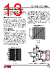
13 / 22 page  LTC1403-1/LTC1403A-1 13 14031fc APPLICATIONS INFORMATION internalreference.Therecommendedrangeforanexternal reference is 2.55V to VDD. An external reference at 2.55V will see a DC quiescent load of 0.75mA and as much as 3mA during conversion. INPUT SPAN VERSUS REFERENCE VOLTAGE The differential input range has a unipolar voltage span that equals the difference between the voltage at the ref- erence buffer output VREF at Pin 3, and the voltage at the ground(ExposedPadGround).Thedifferentialinputrange of the ADC is ±1.25V when using the internal reference. The internal ADC is referenced to these two nodes. This relationship also holds true with an external reference. DIFFERENTIAL INPUTS The LTC1403-1/LTC1403A-1 have a unique differential sample-and-hold circuit that allows inputs from ground to VDD. The ADC will always convert the bipolar differ- ence of AIN+ – AIN–, independent of the common mode voltage at the inputs. The common mode rejection holds up at extremely high frequencies, see Figure 4. The only requirement is that both inputs not go below ground or exceed VDD. Integral nonlinearity errors (INL) and differ- ential nonlinearity errors (DNL) are largely independent of the common mode voltage. However, the offset error will vary. The change in offset error is typically less than 0.1% of the common mode voltage. Figure 5 shows the ideal input/output characteristics for the LTC1403-1/LTC1403A-1. The code transitions occur midway between successive integer LSB values (i.e., 0.5LSB, 1.5LSB, 2.5LSB, FS – 1.5LSB). The output code is 2’s complement with 1LSB = 2.5V/16384 = 153µV for the LTC1403A-1, and 1LSB = 2.5V/4096 = 610µV for the LTC1403-1. The LTC1403A-1 has 1LSB RMS of random white noise. Figure 6a shows the LTC1819 converting a single ended input signal to differential input signals for optimum THD and SFDR performance as shown in the FFT plot (Figure 6b). Figure 4 CMRR vs Frequency FREQUENCY (Hz) 100 0 –20 –40 –60 –80 –100 –120 1k 10k 100k 1M 14031 F04 10M 100M Figure 5 LTC1403-1/LTC1403A-1 Transfer Characteristic INPUT VOLTAGE (V) 14031 F05 011...111 011...110 011...101 100...000 100...001 100...010 FS – 1LSB –FS AIN– LTC1403A-1 AIN+ C1 47pF TO 1000pF 1 R1 51 C3 1µF C5 0.1µF 5V –5V C4 1µF R5 1k 1.5VCM R3 499 R4 499 R6 1k C2 47pF TO 1000pF R2 51 C6 0.1µF VIN 1.25VP-P MAX 1403A F06a U1 1/2 LT1819 U2 1/2 LT1819 Figure 6a. The LT1819 Driving the LTC1403A-1 Differentially |
|
|
Enlace URL |
| ¿ALLDATASHEET es útil para Ud.? [ DONATE ] |
Todo acerca de Alldatasheet | Publicidad | Contáctenos | Política de Privacidad | Enlace a la hoja de datos | Intercambio de Enlaces | Lista de Fabricantes All Rights Reserved©Alldatasheet.com |
| Russian : Alldatasheetru.com | Korean : Alldatasheet.co.kr | Spanish : Alldatasheet.es | French : Alldatasheet.fr | Italian : Alldatasheetit.com Portuguese : Alldatasheetpt.com | Polish : Alldatasheet.pl | Vietnamese : Alldatasheet.vn Indian : Alldatasheet.in | Mexican : Alldatasheet.com.mx | British : Alldatasheet.co.uk | New Zealand : Alldatasheet.co.nz |
|
Family Site : ic2ic.com |
icmetro.com |
 Spanish ▼
 English
 Chinese
 German
 Japanese
 Russian
 Korean
 Spanish
 French
 Italian
 Portuguese
 Polish
 Vietnamese
 Indian
 Mexican
 British
 New Zealand