|
Motor de Búsqueda de Datasheet de Componentes Electrónicos |
|
|
Motor de Búsqueda de Datasheet de Componentes Electrónicos |
|
ADCMP370AKS-R7 Datasheet(PDF) 6 Page - Analog Devices |
|
|
|||||||||||||||||||||||||||||
ADCMP370AKS-R7 Datasheet(HTML) 6 Page - Analog Devices |
|
|
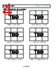
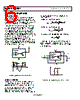
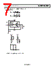
6 / 8 page  ADCMP370/ADCMP371 Preliminary Technical Data Rev. PrB | Page 6 of 8 APPLICATIONS INFORMATION BASIC COMPARATOR In it’s most basic configuration, a comparator can be used to convert an analog input signal to a digital output signal. The analog signal on IN+ is compared to the voltage on IN- and the voltage at OUT is either high or low depending on whether IN+ is at a higher or lower potential than IN-, respectively. The ADCMP370 and ADCMP371 have different digital output structures. The ADCMP370 has an open-drain output stage which requires an external resistor to pull OUT to the logic high voltage level when the output transistor is switched off. This voltage level can be as high as 22V. The pull-up resistor should be large enough to avoid excessive power dissipation, but small enough to switch logic levels reasonably quickly when the comparator output is connected to other digital circuitry. A suitable value would be between 1k Ω and 10kΩ. The ADCMP371 has a push-pull output stage which has an internal PMOS pull-up and therefore doesn’t require an external resistor. Faster switching speeds between low and high rails are possible, but the logic high level is limited to VCC. VIN ADM331 VREF OUT VCC V+ VREF VIN t V+ VOUT 0V Figure 12. Basic Comparator and Input and Output Signals ADDING HYSTERESIS To prevent oscillations at the output caused by noise or slowly moving signals passing the switching threshold, positive feedback can be used to add hysteresis to the differential input. For the non-inverting configuration, shown in figure 13, two resistors are used to create different switching thresholds depending on whether the input signal is increasing or decreasing in magnitude. When the input voltage is increasing, the threshold is above VREF and when it’s decreasing, the threshold is below VREF. The upper input threshold level is given by: () 2 1 2 1 V V REF IN_HI R R V R R CC − + = The lower input threshold level is given by: () 2 2 1 V V REF IN_LO R R R + = The hysteresis is the difference between these voltage levels: 2 1 V V CC IN R R = ∆ In the example in figure 13, resistors R1 and R2 are chosen to give 1V hysteresis about the reference of 2.5V, with VCC=5V. It’s important that RPULL-UP<<RLOAD so that the output high voltage isn’t pulled below VCC. R1=200k ADM331 OUT VCC=5V RLOAD RPULL-UP=5k VIN IN- IN+ VIN_LO VIN_HI VIN VOUT VREF=2.5V R2=1M =2V =3V Figure 13. Non-Inverting Comparator Configuration with Hysteresis ADCMP370 ADCMP370 |
|
|
Enlace URL |
| ¿ALLDATASHEET es útil para Ud.? [ DONATE ] |
Todo acerca de Alldatasheet | Publicidad | Contáctenos | Política de Privacidad | Enlace a la hoja de datos | Intercambio de Enlaces | Lista de Fabricantes All Rights Reserved©Alldatasheet.com |
| Russian : Alldatasheetru.com | Korean : Alldatasheet.co.kr | Spanish : Alldatasheet.es | French : Alldatasheet.fr | Italian : Alldatasheetit.com Portuguese : Alldatasheetpt.com | Polish : Alldatasheet.pl | Vietnamese : Alldatasheet.vn Indian : Alldatasheet.in | Mexican : Alldatasheet.com.mx | British : Alldatasheet.co.uk | New Zealand : Alldatasheet.co.nz |
|
Family Site : ic2ic.com |
icmetro.com |
 Spanish ▼
 English
 Chinese
 German
 Japanese
 Russian
 Korean
 Spanish
 French
 Italian
 Portuguese
 Polish
 Vietnamese
 Indian
 Mexican
 British
 New Zealand