|
Motor de Búsqueda de Datasheet de Componentes Electrónicos |
|
|
Motor de Búsqueda de Datasheet de Componentes Electrónicos |
|
AD8065 Datasheet(PDF) 13 Page - Analog Devices |
|
|
|||||||||||||||||||||||||||||
AD8065 Datasheet(HTML) 13 Page - Analog Devices |
|
|
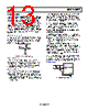
13 / 20 page  Data Sheet AD5547/AD5557 Rev. D | Page 13 of 20 DIGITAL SECTION The AD5547/AD5557 have 16-/14-bit parallel inputs. The devices are double buffered with 16-/14-bit registers. The double buffered feature allows the simultaneous update of several AD5547s/ AD5557s. For the AD5547, the input register is loaded directly from a 16-bit controller bus when WR is brought low. The DAC register is updated with data from the input register when LDAC is brought high. Updating the DAC register updates the DAC output with the new data (see Figure 18). To make both registers transparent, tie WR low and LDAC high. The asynchronous RS pin resets the part to zero scale if MSB = 0 and to midscale if MSB = 1. ESD Protection Circuits All logic input pins contain back-biased ESD protection Zeners connected to ground (DGND) and VDD, as shown in Figure 19. As a result, the voltage level of the logic input should not be greater than the supply voltage. 5kΩ DIGITAL INPUTS DGND VDD Figure 19. Equivalent ESD Protection Circuits Amplifier Selection In addition to offset voltage, the bias current is important in op amp selection for precision current output DACs. A 30 nA input bias current in the op amp contributes to 1 LSB in the full-scale error of the AD5547. The OP1177 and AD8628 op amps are good candidates for the I-to-V conversion. Reference Selection The initial accuracy and rated output of the voltage reference determine the full-span adjustment. The initial accuracy of the reference is usually a secondary concern because it can be trimmed. Figure 25 shows an example of a trimming circuit. The zero-scale error can also be minimized by standard op amp nulling techniques. The voltage reference temperature coefficient (TC) and long- term drift are primary considerations. For example, a 5 V reference with a TC of 5 ppm/°C means the output changes by 25 µV/°C. As a result, a reference operating at 55°C contributes an additional 750 µV full-scale error. Similarly, the same 5 V reference with a ±50 ppm long-term drift means the output may change by ±250 µV over time. Therefore, it is practical to calibrate a system periodically to maintain its optimum precision. PCB LAYOUT, POWER SUPPLY BYPASSING, AND GROUND CONNECTIONS It is a good practice to employ a compact, minimum lead length, PCB layout design. The leads to the input should be as short as possible to minimize IR drop and stray inductance. The PCB metal traces between VREF and RFB should also be matched to minimize gain error. It is also essential to bypass the power supply with quality capacitors for optimum stability. Supply leads to the device should be bypassed with 0.01 µF to 0.1 µF disc or chip ceramic capacitors. Low ESR 1 µF to 10 µF tantalum or electrolytic capacitors should also be applied at the supply in parallel with the ceramic capacitor to minimize transient disturbance and filter out low frequency ripple. To minimize the digital ground bounce, the AD5547/AD5557 DGND terminal should be joined with the AGND terminal at a single point. Figure 20 illustrates the basic supply bypassing configuration and AGND/DGND connection for the AD5547/AD5557. VDD AGND DGND C1 C2 5V + – 1µF 0.1µF AD5547/AD5557 Figure 20. Power Supply Bypassing |
|
|
Enlace URL |
| ¿ALLDATASHEET es útil para Ud.? [ DONATE ] |
Todo acerca de Alldatasheet | Publicidad | Contáctenos | Política de Privacidad | Enlace a la hoja de datos | Intercambio de Enlaces | Lista de Fabricantes All Rights Reserved©Alldatasheet.com |
| Russian : Alldatasheetru.com | Korean : Alldatasheet.co.kr | Spanish : Alldatasheet.es | French : Alldatasheet.fr | Italian : Alldatasheetit.com Portuguese : Alldatasheetpt.com | Polish : Alldatasheet.pl | Vietnamese : Alldatasheet.vn Indian : Alldatasheet.in | Mexican : Alldatasheet.com.mx | British : Alldatasheet.co.uk | New Zealand : Alldatasheet.co.nz |
|
Family Site : ic2ic.com |
icmetro.com |
 Spanish ▼
 English
 Chinese
 German
 Japanese
 Russian
 Korean
 Spanish
 French
 Italian
 Portuguese
 Polish
 Vietnamese
 Indian
 Mexican
 British
 New Zealand