|
Motor de Búsqueda de Datasheet de Componentes Electrónicos |
|
|
Motor de Búsqueda de Datasheet de Componentes Electrónicos |
|
AD629ARZ-R7 Datasheet(PDF) 9 Page - Analog Devices |
|
|
|||||||||||||||||||||||||||||
AD629ARZ-R7 Datasheet(HTML) 9 Page - Analog Devices |
|
|
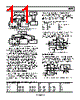
9 / 16 page  AD629 Rev. B | Page 9 of 16 THEORY OF OPERATION The AD629 is a unity gain, differential-to-single-ended amplifier (diff amp) that can reject extremely high common- mode signals (in excess of 270 V with 15 V supplies). It consists of an operational amplifier (op amp) and a resistor network. To achieve high common-mode voltage range, an internal resistor divider (Pin 3 or Pin 5) attenuates the noninverting signal by a factor of 20. Other internal resistors (Pin 1, Pin 2, and the feedback resistor) restore the gain to provide a differential gain of unity. The complete transfer function equals VOUT = V (+IN) − V (−IN) Laser wafer trimming provides resistor matching so that common-mode signals are rejected while differential input signals are amplified. To reduce output drift, the op amp uses super beta transistors in its input stage. The input offset current and its associated temperature coefficient contribute no appreciable output voltage offset or drift, which has the added benefit of reducing voltage noise because the corner where 1/f noise becomes dominant is below 5 Hz. To reduce the dependence of gain accuracy on the op amp, the open-loop voltage gain of the op amp exceeds 20 million, and the PSRR exceeds 140 dB. 1 2 3 4 8 7 6 5 21.1kΩ 380kΩ 380kΩ 380kΩ 20kΩ REF(–) –IN +IN –VS NC +VS OUTPUT REF(+) AD629 NC = NO CONNECT Figure 29. Functional Block Diagram |
|
|
Enlace URL |
| ¿ALLDATASHEET es útil para Ud.? [ DONATE ] |
Todo acerca de Alldatasheet | Publicidad | Contáctenos | Política de Privacidad | Enlace a la hoja de datos | Intercambio de Enlaces | Lista de Fabricantes All Rights Reserved©Alldatasheet.com |
| Russian : Alldatasheetru.com | Korean : Alldatasheet.co.kr | Spanish : Alldatasheet.es | French : Alldatasheet.fr | Italian : Alldatasheetit.com Portuguese : Alldatasheetpt.com | Polish : Alldatasheet.pl | Vietnamese : Alldatasheet.vn Indian : Alldatasheet.in | Mexican : Alldatasheet.com.mx | British : Alldatasheet.co.uk | New Zealand : Alldatasheet.co.nz |
|
Family Site : ic2ic.com |
icmetro.com |
 Spanish ▼
 English
 Chinese
 German
 Japanese
 Russian
 Korean
 Spanish
 French
 Italian
 Portuguese
 Polish
 Vietnamese
 Indian
 Mexican
 British
 New Zealand