 |
Motor de Búsqueda de Datasheet de Componentes Electrónicos |
|
|
Motor de Búsqueda de Datasheet de Componentes Electrónicos |
|
The question interval is too short.
Please try again in a few seconds.

Hello, Please ask a question about SMC Datasheet
# Example questions:
➢ G., sot-23, to252). what kind of information is consistently provided for each package type?
➢ Identify three different package types that have a 'y' dimension value of approximately 0mm.
➢ What is the primary purpose of the information presented?
| Part No. | SMC |
| Manufacturer | DIODES |
| Size | 174 Kbytes |
| Pages | 12 pages |
| Description | SUGGESTED PAD LAYOUT |

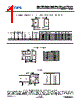

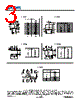
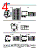
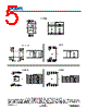


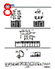
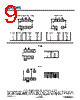
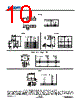
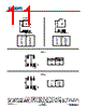


1. Package Types Covered:
The catalog covers a wide range of package types, categorized roughly by complexity and size. This includes:
️· Small Outline Packages (SOPs): SC-74R, SOT-26, SOT-363, SOT-563. These are common surface-mount packages.
️· Small Component Outline Packages (SCOs): SOT-25, SOT-353
️· Very Small Packages: SOT-953, SOT-666
️· Power Packages: TO252-3L (DPAK), TO263-3L (D2PAK), TO252-4L
️· Standard Outline Packages: SOT-89-3L and SOT-89-5L
️· Mini/Micro Packages: SOT-523, SOT-323, SOT23, SC-59, SOT-23F
️· Other: SOT-963
2. Dimensions Provided:
For each package type, the document lists several key dimensions:
️· Z: Height or thickness of the package.
️· G: Gauge (width of the lead spacing).
️· X, X1, X2: Horizontal distances related to the package width.
️· Y, Y1, Y2, Y3, Y4: Vertical distances related to the package height.
️· C: Distance related to lead spacing and body placement.
️· E: Often a distance related to lead spacing in power packages.
️· c, c1: Related to spacing and center alignment in larger packages.
3. Purpose:
The primary purpose of this document is to assist PCB designers in creating accurate land patterns for Diodes Incorporated semiconductor components. Using these suggested land patterns helps ensure:
️· Proper Component Placement: Components are positioned correctly on the PCB.
️· Reliable Soldering: Soldering joints are robust and provide good electrical and mechanical connections.
️· Manufacturing Consistency: Land patterns are consistent across different PCB designs and manufacturing runs.
4. Important Note:
The document explicitly states that these are "suggested" land patterns. Designers should always verify the actual component dimensions using the component datasheet and adjust the land pattern as needed to suit the specific application and manufacturing process.
In essence, this is a reference guide for PCB layout engineers working with Diodes Incorporated components, aimed at creating reliable and manufacturable PCB designs.
1. Package Types Covered:
The catalog covers a wide range of package types, categorized roughly by complexity and size. This includes:
️· Small Outline Packages (SOPs): SC-74R, SOT-26, SOT-363, SOT-563. These are common surface-mount packages.
️· Small Component Outline Packages (SCOs): SOT-25, SOT-353
️· Very Small Packages: SOT-953, SOT-666
️· Power Packages: TO252-3L (DPAK), TO263-3L (D2PAK), TO252-4L
️· Standard Outline Packages: SOT-89-3L and SOT-89-5L
️· Mini/Micro Packages: SOT-523, SOT-323, SOT23, SC-59, SOT-23F
️· Other: SOT-963
2. Dimensions Provided:
For each package type, the document lists several key dimensions:
️· Z: Height or thickness of the package.
️· G: Gauge (width of the lead spacing).
️· X, X1, X2: Horizontal distances related to the package width.
️· Y, Y1, Y2, Y3, Y4: Vertical distances related to the package height.
️· C: Distance related to lead spacing and body placement.
️· E: Often a distance related to lead spacing in power packages.
️· c, c1: Related to spacing and center alignment in larger packages.
3. Purpose:
The primary purpose of this document is to assist PCB designers in creating accurate land patterns for Diodes Incorporated semiconductor components. Using these suggested land patterns helps ensure:
️· Proper Component Placement: Components are positioned correctly on the PCB.
️· Reliable Soldering: Soldering joints are robust and provide good electrical and mechanical connections.
️· Manufacturing Consistency: Land patterns are consistent across different PCB designs and manufacturing runs.
4. Important Note:
The document explicitly states that these are "suggested" land patterns. Designers should always verify the actual component dimensions using the component datasheet and adjust the land pattern as needed to suit the specific application and manufacturing process.
In essence, this is a reference guide for PCB layout engineers working with Diodes Incorporated components, aimed at creating reliable and manufacturable PCB designs.
| Part No. | SMC |
| Manufacturer | DIODES |
| Size | 174 Kbytes |
| Pages | 12 pages |
| Description | SUGGESTED PAD LAYOUT |
| ¿ALLDATASHEET es útil para Ud.? [ DONATE ] |
Todo acerca de Alldatasheet | Publicidad | Contáctenos | Política de Privacidad | Enlace a la hoja de datos | Intercambio de Enlaces | Lista de Fabricantes All Rights Reserved©Alldatasheet.com |
| Russian : Alldatasheetru.com | Korean : Alldatasheet.co.kr | Spanish : Alldatasheet.es | French : Alldatasheet.fr | Italian : Alldatasheetit.com Portuguese : Alldatasheetpt.com | Polish : Alldatasheet.pl | Vietnamese : Alldatasheet.vn Indian : Alldatasheet.in | Mexican : Alldatasheet.com.mx | British : Alldatasheet.co.uk | New Zealand : Alldatasheet.co.nz |
|
Family Site : ic2ic.com |
icmetro.com |
 Spanish ▼
  English
 Chinese
 German
 Japanese
 Russian
 Korean
 French
 Italian
 Portuguese
 Polish
 Vietnamese
 Indian
 Mexican
 British
 New Zealand